STB50NF25 STMicroelectronics, STB50NF25 Datasheet - Page 4
STB50NF25
Manufacturer Part Number
STB50NF25
Description
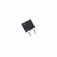
MOSFET N-CH 250V 45A D2PAK
Manufacturer
STMicroelectronics
Series
STripFET™r
Datasheet
1.STB50NF25.pdf
(14 pages)
Specifications of STB50NF25
Fet Type
MOSFET N-Channel, Metal Oxide
Fet Feature
Standard
Rds On (max) @ Id, Vgs
69 mOhm @ 22A, 10V
Drain To Source Voltage (vdss)
250V
Current - Continuous Drain (id) @ 25° C
45A
Vgs(th) (max) @ Id
4V @ 250µA
Gate Charge (qg) @ Vgs
68.2nC @ 10V
Input Capacitance (ciss) @ Vds
2670pF @ 25V
Power - Max
160W
Mounting Type
Surface Mount
Package / Case
D²Pak, TO-263 (2 leads + tab)
Configuration
Single
Transistor Polarity
N-Channel
Resistance Drain-source Rds (on)
0.069 Ohm @ 10 V
Drain-source Breakdown Voltage
250 V
Gate-source Breakdown Voltage
+/- 20 V
Continuous Drain Current
45 A
Power Dissipation
160000 mW
Maximum Operating Temperature
+ 150 C
Mounting Style
SMD/SMT
Minimum Operating Temperature
- 55 C
Continuous Drain Current Id
22A
Drain Source Voltage Vds
250V
On Resistance Rds(on)
55mohm
Rds(on) Test Voltage Vgs
10V
Threshold Voltage Vgs Typ
3V
Rohs Compliant
Yes
Lead Free Status / RoHS Status
Lead free / RoHS Compliant
Other names
497-7949-2
STB50NF25
STB50NF25
Available stocks
Company
Part Number
Manufacturer
Quantity
Price
Company:

Part Number:
STB50NF25
Manufacturer:
ST
Quantity:
12 500


Electrical characteristics
2
4/14
Electrical characteristics
(T
Table 5.
Table 6.
1. Pulsed: pulse duration=300µs, duty cycle 1.5%
V
Symbol
Symbol
R
CASE
V
(BR)DSS
g
C
I
I
C
DS(on)
C
Q
Q
GS(th)
GSS
fs
R
DSS
Q
oss
rss
iss
gd
gs
G
g
(1)
=25°C unless otherwise specified)
Forward transconductance
Input capacitance
Output capacitance
Reverse transfer
capacitance
Total gate charge
Gate-source charge
Gate-drain charge
Gate input resistance
Drain-source breakdown
voltage
Zero gate voltage drain
current (V
Gate body leakage current
(V
Gate threshold voltage
Static drain-source on
resistance
On/off states
Dynamic
DS
= 0)
Parameter
Parameter
GS
= 0)
V
V
V
V
V
(see Figure 14)
f=1 MHz Gate Bias, Bias=0
Test signal level=20 mV
open drain
I
V
V
V
V
V
D
DS
DS
GS
DD
GS
DS
DS
GS
DS
GS
= 1 mA, V
=0
=200 V, I
= V
= 10 V, I
=10 V, I
=25 V, f=1 MHz,
=10 V
= Max rating,
= Max rating @125 °C
= ±20 V
Test conditions
Test conditions
GS
, I
D
D
D
GS
D
= 22 A
= 22 A
= 250 µA
= 45 A
= 0
Min.
Min.
STB50NF25 - STP50NF25
250
2
0.055
Typ.
2670
Typ.
70.5
68.2
12.2
33.4
465
1.1
20
3
0.069
Max.
±
Max.
100
10
1
4
Unit
Unit
µA
µA
nA
nC
nC
nC
pF
pF
pF
V
V
Ω
S
Ω
Related parts for STB50NF25
Image
Part Number
Description
Manufacturer
Datasheet
Request
R

Part Number:
Description:
STMicroelectronics [RIPPLE-CARRY BINARY COUNTER/DIVIDERS]
Manufacturer:
STMicroelectronics
Datasheet:
Part Number:
Description:
STMicroelectronics [LIQUID-CRYSTAL DISPLAY DRIVERS]
Manufacturer:
STMicroelectronics
Datasheet:

Part Number:
Description:
BOARD EVAL FOR MEMS SENSORS
Manufacturer:
STMicroelectronics
Datasheet:
Part Number:
Description:
NPN TRANSISTOR POWER MODULE
Manufacturer:
STMicroelectronics
Datasheet:
Part Number:
Description:
TURBOSWITCH ULTRA-FAST HIGH VOLTAGE DIODE
Manufacturer:
STMicroelectronics
Datasheet:
Part Number:
Description:
Manufacturer:
STMicroelectronics
Datasheet:
Part Number:
Description:
DIODE / SCR MODULE
Manufacturer:
STMicroelectronics
Datasheet:
Part Number:
Description:
DIODE / SCR MODULE
Manufacturer:
STMicroelectronics
Datasheet:
Part Number:
Description:
Search -----> STE16N100
Manufacturer:
STMicroelectronics
Datasheet:
Part Number:
Description:
Search ---> STE53NA50
Manufacturer:
STMicroelectronics
Datasheet:
Part Number:
Description:
NPN Transistor Power Module
Manufacturer:
STMicroelectronics
Datasheet:
Part Number:
Description:
DIODE / SCR MODULE
Manufacturer:
STMicroelectronics
Datasheet: