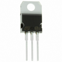
STP80NF03L-04 STMicroelectronics, STP80NF03L-04 Datasheet

STP80NF03L-04
Specifications of STP80NF03L-04
Available stocks
Related parts for STP80NF03L-04
STP80NF03L-04 Summary of contents
Page 1
... DC-DC & DC-AC CONVERTERS AUTOMOTIVE ENVIRONMENT (INJECTION,ABS, AIR-BAG ,LAMPDRIVERS Etc.) ORDERING INFORMATION SALES TYPE STP80NF03L January 2004 N-CHANNEL 30V - 0.004 R I DS(on) D < 0.0045 80 A MARKING PACKAGE P80NF03L TO-220 . STP80NF03L - 80A TO-220 STripFET™ II MOSFET TO-220 INTERNAL SCHEMATIC DIAGRAM PACKAGING TUBE 1/8 ...
Page 2
... STP80NF03L ABSOLUTE MAXIMUM RATINGS Symbol V Drain-source Voltage ( Drain-gate Voltage (R DGR V Gate-source Voltage GS I (#) Drain Current (continuous (#) Drain Current (continuous Drain Current (pulsed Total Dissipation at T TOT Derating Factor dv/dt (1) Peak Diode Recovery Voltage Slope T Storage Temperature stg T Max. Operating Junction Temperature j (#) Current Limited by Package ...
Page 3
... G GS (Resistive Load, Figure clamp 4 4. (Inductive Load, Figure 5) Test Conditions di/dt = 100 A/µ 150° (see test circuit, Figure 5) STP80NF03L Min. Typ. Max. Unit 50 S 5500 pF 1670 pF 290 pF Min. Typ. Max. Unit 30 ns 270 ns 85 110 Min. Typ. Max. Unit ...
Page 4
... STP80NF03L Safe Operating Area Output Characteristics Transconductance 4/8 Thermal Impedance Transfer Characteristics Static Drain-source On Resistance ...
Page 5
... Gate Charge vs Gate-source Voltage Normalized Gate Threshold Voltage vs Temp. Source-drain Diode Forward Characteristics Capacitance Variations Normalized On Resistance vs Temperature NormalizedBreakdownVoltage vs Temperature STP80NF03L 5/8 ...
Page 6
... STP80NF03L Fig. 1: Unclamped Inductive Load Test Circuit Fig. 3: Switching Times Test Circuit For Resistive Load Fig. 5: Test Circuit For Inductive Load Switching And Diode Recovery Times 6/8 Fig. 2: Unclamped Inductive Waveform Fig. 4: Gate Charge test Circuit ...
Page 7
... STP80NF03L MAX. 0.181 0.034 0.066 0.027 0.620 0.409 0.106 0.202 0.052 0.256 0.107 0.551 0.154 0.151 0.116 7/8 ...
Page 8
... STP80NF03L Information furnished is believed to be accurate and reliable. However, STMicroelectronics assumes no responsibility for the consequences of use of such information nor for any infringement of patents or other rights of third parties which may result from its use. No license is granted by implication or otherwise under any patent or patent rights of STMicroelectronics. Specifications mentioned in this publication are subject to change without notice ...


