STB50N25M5 STMicroelectronics, STB50N25M5 Datasheet - Page 3
STB50N25M5
Manufacturer Part Number
STB50N25M5
Description
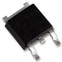
MOSFET N-CH 250V 28A D2PAK
Manufacturer
STMicroelectronics
Series
MDmesh™r
Datasheet
1.STB50N25M5.pdf
(13 pages)
Specifications of STB50N25M5
Fet Type
MOSFET N-Channel, Metal Oxide
Fet Feature
Standard
Rds On (max) @ Id, Vgs
65 mOhm @ 14A, 10V
Drain To Source Voltage (vdss)
250V
Current - Continuous Drain (id) @ 25° C
28A
Vgs(th) (max) @ Id
5V @ 100µA
Gate Charge (qg) @ Vgs
44nC @ 10V
Input Capacitance (ciss) @ Vds
1700pF @ 50V
Power - Max
110W
Mounting Type
Surface Mount
Package / Case
D²Pak, TO-263 (2 leads + tab)
Transistor Polarity
N Channel
Continuous Drain Current Id
14A
Drain Source Voltage Vds
250V
On Resistance Rds(on)
55mohm
Rds(on) Test Voltage Vgs
10V
Threshold Voltage Vgs Typ
4V
Rohs Compliant
Yes
Lead Free Status / RoHS Status
Lead free / RoHS Compliant
Other names
497-10024-2
Available stocks
Company
Part Number
Manufacturer
Quantity
Price


STB50N25M5
1
Electrical ratings
Table 2.
1. Pulse width limited by safe operating area
2. I
Table 3.
Symbol
Symbol
R
dv/dt
R
I
P
DM
thj-case
V
E
T
thj-pcb
I
SD
T
T
I
I
TOT
AR
GS
stg
AS
D
D
J
J
(1)
(2)
≤ 28 A, di/dt ≤ 400 A/µs, V
Gate- source voltage
Drain current (continuous) at T
Drain current (continuous) at T
Drain current (pulsed)
Total dissipation at T
Avalanche current, repetitive or not-repetitive
(pulse width limited by T
Single pulse avalanche energy
(starting T
Peak diode recovery voltage slope
Operating junction temperature
Storage temperature
Thermal resistance junction-case max
Thermal resistance junction-pcb max
Maximum lead temperature for soldering purpose
Absolute maximum ratings
Thermal data
J
= 25 °C, I
Parameter
Parameter
C
D
Doc ID 15923 Rev 1
Peak
= 25 °C
= I
J
max)
AR
< V
, V
(BR)DSS
C
C
DD
= 25 °C
= 100 °C
= 50 V)
-55 to 150
Value
Value
0.31
112
110
350
300
15
25
28
18
30
9
Electrical ratings
°C/W
°C/W
°C/W
V/ns
Unit
Unit
mJ
°C
W
V
A
A
A
A
3/13
Related parts for STB50N25M5
Image
Part Number
Description
Manufacturer
Datasheet
Request
R

Part Number:
Description:
STMicroelectronics [RIPPLE-CARRY BINARY COUNTER/DIVIDERS]
Manufacturer:
STMicroelectronics
Datasheet:
Part Number:
Description:
STMicroelectronics [LIQUID-CRYSTAL DISPLAY DRIVERS]
Manufacturer:
STMicroelectronics
Datasheet:

Part Number:
Description:
BOARD EVAL FOR MEMS SENSORS
Manufacturer:
STMicroelectronics
Datasheet:
Part Number:
Description:
NPN TRANSISTOR POWER MODULE
Manufacturer:
STMicroelectronics
Datasheet:
Part Number:
Description:
TURBOSWITCH ULTRA-FAST HIGH VOLTAGE DIODE
Manufacturer:
STMicroelectronics
Datasheet:
Part Number:
Description:
Manufacturer:
STMicroelectronics
Datasheet:
Part Number:
Description:
DIODE / SCR MODULE
Manufacturer:
STMicroelectronics
Datasheet:
Part Number:
Description:
DIODE / SCR MODULE
Manufacturer:
STMicroelectronics
Datasheet:
Part Number:
Description:
Search -----> STE16N100
Manufacturer:
STMicroelectronics
Datasheet:
Part Number:
Description:
Search ---> STE53NA50
Manufacturer:
STMicroelectronics
Datasheet:
Part Number:
Description:
NPN Transistor Power Module
Manufacturer:
STMicroelectronics
Datasheet:
Part Number:
Description:
DIODE / SCR MODULE
Manufacturer:
STMicroelectronics
Datasheet: