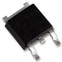
STB50N25M5 STMicroelectronics, STB50N25M5 Datasheet - Page 4

STB50N25M5
Manufacturer Part Number
STB50N25M5
Description
MOSFET N-CH 250V 28A D2PAK
Manufacturer
STMicroelectronics
Series
MDmesh™r
Datasheet
1.STB50N25M5.pdf
(13 pages)
Specifications of STB50N25M5
Fet Type
MOSFET N-Channel, Metal Oxide
Fet Feature
Standard
Rds On (max) @ Id, Vgs
65 mOhm @ 14A, 10V
Drain To Source Voltage (vdss)
250V
Current - Continuous Drain (id) @ 25° C
28A
Vgs(th) (max) @ Id
5V @ 100µA
Gate Charge (qg) @ Vgs
44nC @ 10V
Input Capacitance (ciss) @ Vds
1700pF @ 50V
Power - Max
110W
Mounting Type
Surface Mount
Package / Case
D²Pak, TO-263 (2 leads + tab)
Transistor Polarity
N Channel
Continuous Drain Current Id
14A
Drain Source Voltage Vds
250V
On Resistance Rds(on)
55mohm
Rds(on) Test Voltage Vgs
10V
Threshold Voltage Vgs Typ
4V
Rohs Compliant
Yes
Lead Free Status / RoHS Status
Lead free / RoHS Compliant
Other names
497-10024-2
Available stocks
Company
Part Number
Manufacturer
Quantity
Price
Electrical characteristics
2
4/13
Electrical characteristics
(Tcase =25°C unless otherwise specified)
Table 4.
Table 5.
1. C
2. C
V
Symbol
Symbol
C
R
C
V
(BR)DSS
to 80% V
to 80% V
C
o(er)
I
I
C
DS(on)
C
o(tr)
Q
GS(th)
Q
GSS
DSS
Q
R
o(er)
o(tr)
oss
iss
rss
gs
gd
g
g
(2)
(1)
is a constant capacitance value that gives the same charging time as C
is a constant capacitance value that gives the same stored energy as C
DSS
DSS
Input capacitance
Output capacitance
Reverse transfer
capacitance
Equivalent output
capacitance energy
related
Equivalent output
capacitance time
related
Gate input resistance
Total gate charge
Gate-source charge
Gate-drain charge
Drain-source
breakdown voltage
Zero gate voltage
drain current (V
Gate-body leakage
current (V
Gate threshold voltage V
Static drain-source on-
resistance
On /off states
Dynamic
Parameter
Parameter
DS
= 0)
GS
= 0)
Doc ID 15923 Rev 1
V
V
V
V
V
V
f=1 MHz open drain
V
V
(see Figure 15)
I
V
V
V
V
D
DS
GS
GS
(BR)DSS
GS
(BR)DSS
DD
GS
DS
DS
GS
DS
GS
= 1 mA, V
= Max rating
= Max rating, T
= 50 V, f = 1 MHz,
= 0
= 0, V
= 0, V
= 10 V
= ± 25 V
= V
= 10 V, I
= 200 V, I
Test conditions
Test conditions
GS
DS
DS
, I
GS
D
D
= 0 to 80%
= 0 to 80%
D
= 100 µA
= 14 A
= 0
= 28 A,
C
=125 °C
Min.
Min.
oss
250
oss
3
-
-
-
-
-
while V
while V
0.055
1700
Typ.
Typ.
100
171
1.8
15
89
44
10
23
DS
DS
4
is rising from 0
is rising from 0
STB50N25M5
0.065
Max.
Max.
100
100
1
5
-
-
-
-
-
Unit
Unit
nC
nC
nC
µA
µA
nA
pF
pF
pF
pF
pF
Ω
Ω
V
V


