STB160N75F3 STMicroelectronics, STB160N75F3 Datasheet
STB160N75F3
Specifications of STB160N75F3
STB160N75F3
Available stocks


Related parts for STB160N75F3


STB160N75F3 Summary of contents
Page 1
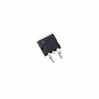
... STripFET™ Power MOSFET R DS(on (max.) (1) 3.7 mΩ 120 A (1) 4 mΩ 120 A (1) 4 mΩ 120 A Figure 1. Marking 160N75F3 160N75F3 160N75F3 Rev 2 STB160N75F3 TO-220 TO-247 3 1 D²PAK Internal schematic diagram Package Packaging D²PAK Tape & reel TO-220 Tube TO-247 Tube 2 PAK 3 ...
Page 2
... Electrical characteristics (curves) 3 Test circuit 4 Package mechanical data . . . . . . . . . . . . . . . . . . . . . . . . . . . . . . . . . . . . 10 5 Packaging mechanical data . . . . . . . . . . . . . . . . . . . . . . . . . . . . . . . . . . 14 6 Revision history . . . . . . . . . . . . . . . . . . . . . . . . . . . . . . . . . . . . . . . . . . . 15 2/16 STB160N75F3 - STP160N75F3 - STW160N75F3 . . . . . . . . . . . . . . . . . . . . . . . . . . . . . . . . . . . . . . . . . . . . . . . . ...
Page 3
... STB160N75F3 - STP160N75F3 - STW160N75F3 1 Electrical ratings Table 2. Absolute maximum ratings Symbol V Drain-source voltage ( Gate-source voltage GS (1) I Drain current (continuous (1) I Drain current (continuous (2) I Drain current (pulsed Total dissipation at T TOT Derating factor (3) Peak diode recovery voltage slope dv/dt (4) E Single pulse avalanche energy ...
Page 4
... DS(on) resistance Table 5. Dynamic Symbol Input capacitance C iss Output capacitance C oss Reverse transfer C rss capacitance Q Total gate charge g Q Gate-source charge gs Gate-drain charge Q gd 4/16 STB160N75F3 - STP160N75F3 - STW160N75F3 Test conditions I = 250µ Max rating Max rating,@125° ±20V 250µ ...
Page 5
... STB160N75F3 - STP160N75F3 - STW160N75F3 Table 6. Switching times Symbol t d(on) Turn-on delay time t Rise time r t Turn-off delay time d(off) Fall time t f Table 7. Source drain diode Symbol I Source-drain current SD (1) Source-drain current (pulsed) I SDM (2) Forward on voltage Reverse recovery time rr Q Reverse recovery charge ...
Page 6
... Electrical characteristics 2.1 Electrical characteristics (curves) Figure 2. Safe operating area for TO-220 / TO-247 Figure 4. Safe operating area for D²PAK Figure 6. Output characteristics 6/16 STB160N75F3 - STP160N75F3 - STW160N75F3 Figure 3. Thermal impedance for TO-220 / TO-247 Figure 5. Thermal impedance for D²PAK Figure 7. Transfer characteristics ...
Page 7
... STB160N75F3 - STP160N75F3 - STW160N75F3 Figure 8. Normalized BV Figure 10. Gate charge vs gate-source voltage Figure 11. Capacitance variations Figure 12. Normalized gate threshold voltage vs temperature vs temperature Figure 9. DSS Figure 13. Normalized on resistance vs Electrical characteristics Static drain-source on resistance temperature 7/16 ...
Page 8
... Electrical characteristics Figure 14. Source-drain diode forward characteristics 8/16 STB160N75F3 - STP160N75F3 - STW160N75F3 ...
Page 9
... STB160N75F3 - STP160N75F3 - STW160N75F3 3 Test circuit Figure 15. Switching times test circuit for resistive load Figure 17. Test circuit for inductive load switching and diode recovery times Figure 19. Unclamped inductive waveform Figure 16. Gate charge test circuit Figure 18. Unclamped inductive load test circuit Figure 20. Switching time waveform ...
Page 10
... These packages have a Lead-free second level interconnect. The category of second level interconnect is marked on the package and on the inner box label, in compliance with JEDEC Standard JESD97. The maximum ratings related to soldering conditions are also marked on the inner box label. ECOPACK trademark. ECOPACK specifications are available at: 10/16 STB160N75F3 - STP160N75F3 - STW160N75F3 www.st.com ...
Page 11
... STB160N75F3 - STP160N75F3 - STW160N75F3 Dim L20 L30 ∅P Q TO-220 mechanical data mm Min Typ Max 4.40 4.60 0.61 0.88 1.14 1.70 0.49 0.70 15.25 15.75 1.27 10 10.40 2.40 2.70 4.95 5.15 1.23 1.32 6.20 6.60 2.40 2. 3.50 3.93 16.40 28.90 3.75 3.85 2.65 2 ...
Page 12
... Package mechanical data DIM øP øR S 12/16 STB160N75F3 - STP160N75F3 - STW160N75F3 TO-247 MECHANICAL DATA mm. MIN. TYP MAX. 4.85 5.15 2.20 2.60 1.0 1.40 2.0 2.40 3.0 3.40 0.40 0.80 19.85 20.15 15.45 15.75 5.45 14.20 14.80 3.70 4.30 18.50 3.55 3.65 4.50 5 ...
Page 13
... STB160N75F3 - STP160N75F3 - STW160N75F3 Dim Min A 4.4 A1 2.49 A2 0.03 B 0.7 B2 1.14 C 0.45 C2 1. 1.27 L3 1 0° D²PAK mechanical data mm Typ Max Min 4.6 0.173 2.69 0.098 0.23 0.001 0.93 0.027 1.7 0.044 0.6 0.017 1.36 0.048 9.35 0.352 8 10.4 0.393 8 ...
Page 14
... P2 1.9 2 0.25 0.35 0.0098 0.0137 W 23.7 24 sales type 14/16 STB160N75F3 - STP160N75F3 - STW160N75F3 TAPE AND REEL SHIPMENT inch MIN. MAX. 0.413 0.421 0.618 0.626 0.059 0.063 0.062 0.063 0.065 0.073 0.449 0.456 0.189 0.197 0.153 0.161 0.468 0.476 0.075 0.082 1 ...
Page 15
... STB160N75F3 - STP160N75F3 - STW160N75F3 6 Revision history Table 8. Document revision history Date 07-Feb-2007 02-Oct-2007 Revision 1 First release 2 New section has been added: Revision history Changes Electrical characteristics (curves) 15/16 ...
Page 16
... Australia - Belgium - Brazil - Canada - China - Czech Republic - Finland - France - Germany - Hong Kong - India - Israel - Italy - Japan - Malaysia - Malta - Morocco - Singapore - Spain - Sweden - Switzerland - United Kingdom - United States of America 16/16 STB160N75F3 - STP160N75F3 - STW160N75F3 Please Read Carefully: © 2007 STMicroelectronics - All rights reserved STMicroelectronics group of companies www ...