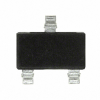
AO3409 Alpha & Omega Semiconductor Inc, AO3409 Datasheet
Home Discrete Semiconductor Products MOSFETs, GaNFETs - Single AO3409
Manufacturer Part Number
AO3409
Description
MOSFET P-CH -30V -2.6A SOT23
Manufacturer
Alpha & Omega Semiconductor Inc
Fet Type
MOSFET P-Channel, Metal Oxide
Fet Feature
Logic Level Gate
Rds On (max) @ Id, Vgs
130 mOhm @ 2.6A, 10V
Drain To Source Voltage (vdss)
30V
Current - Continuous Drain (id) @ 25° C
2.6A
Vgs(th) (max) @ Id
3V @ 250µA
Gate Charge (qg) @ Vgs
9nC @ 10V
Input Capacitance (ciss) @ Vds
370pF @ 15V
Power - Max
1.4W
Mounting Type
Surface Mount
Package / Case
SOT-23-3, TO-236-3, Micro3™, SSD3, SST3
Lead Free Status / RoHS Status
Lead free / RoHS Compliant
Available stocks
Alpha & Omega Semiconductor, Ltd.
Absolute Maximum Ratings T
Parameter
Drain-Source Voltage
Gate-Source Voltage
Continuous Drain
Current
Pulsed Drain Current
Power Dissipation
Junction and Storage Temperature Range
Thermal Characteristics
Parameter
Maximum Junction-to-Ambient
Maximum Junction-to-Ambient
Maximum Junction-to-Lead
General Description
The AO3409/L uses advanced trench technology to
provide excellent R
device is suitable for use as a load switch or in PWM
applications. AO3409 and AO3409L are electrically
identical.
-RoHS Compliant
-AO3409L is Halogen Free
AO3409
P-Channel Enhancement Mode Field Effect Transistor
A
A
DS(ON)
G
S
B
T
T
T
T
(SOT-23)
Top View
A
A
A
A
TO-236
=25° C
=70° C
=25° C
=70° C
and low gate charge. This
C
A
A
A
D
=25° C unless otherwise noted
Steady-State
Steady-State
t ≤ 10s
Symbol
V
V
I
I
P
T
D
DM
J
DS
GS
D
, T
STG
Symbol
Features
V
I
R
R
G
R
R
D
DS
DS(ON)
DS(ON)
= -2.6 A (V
JA
JL
(V) = -30V
< 130m
< 200m
D
S
Maximum
-55 to 150
-2.6
-2.2
Typ
±20
100
-30
-20
1.4
70
63
GS
1
= -10V)
(V
(V
GS
GS
= -10V)
= -4.5V)
Max
125
90
80
Units
Units
° C/W
° C/W
° C/W
° C
W
V
V
A
www.aosmd.com
Related parts for AO3409
AO3409 Summary of contents
... AO3409 P-Channel Enhancement Mode Field Effect Transistor General Description The AO3409/L uses advanced trench technology to provide excellent R and low gate charge. This DS(ON) device is suitable for use as a load switch or in PWM applications. AO3409 and AO3409L are electrically identical. -RoHS Compliant ...
... AO3409 Electrical Characteristics (T =25° C unless otherwise noted) J Symbol Parameter STATIC PARAMETERS BV Drain-Source Breakdown Voltage DSS I Zero Gate Voltage Drain Current DSS I Gate-Body leakage current GSS V Gate Threshold Voltage GS(th state drain current D(ON) R Static Drain-Source On-Resistance DS(ON) g Forward Transconductance FS V Diode Forward Voltage ...
... AO3409 TYPICAL ELECTRICAL AND THERMAL CHARACTERISTICS 20 -10V (Volts) DS Fig 1: On-Region Characteristics 250 200 150 100 (A) D Figure 3: On-Resistance vs. Drain Current and Gate Voltage 300 250 200 150 100 (Volts) GS Figure 5: On-Resistance vs. Gate-Source Voltage Alpha & Omega Semiconductor, Ltd. 10 -8V 8 -6V 6 -5.5V ...
... AO3409 TYPICAL ELECTRICAL AND THERMAL CHARACTERISTICS 10 V =-15V =-2. (nC) g Figure 7: Gate-Charge Characteristics 100.0 T =150°C J(Max) T =25° 10.0 DS(ON) limited 0.1s 1.0 1s 10s 0.1 0 (Volts) DS Figure 9: Maximum Forward Biased Safe Operating Area (Note =90°C 0.1 Single Pulse 0.01 ...
Related keywords
ao3409 ao3407a ao3407 ao3406 ao3404 ao3403 ao3401a ao3401 AO3409 datasheet AO3409 data sheet AO3409 pdf datasheet AO3409 component AO3409 part AO3409 distributor AO3409 RoHS AO3409 datasheet download


