IPB100N06S3L-03 Infineon Technologies, IPB100N06S3L-03 Datasheet
IPB100N06S3L-03
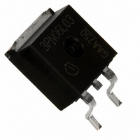
Specifications of IPB100N06S3L-03
IPB100N06S3L-03XTINTR
IPB100N06S3L-03XTINTR
IPB100N06S3L03XT
SP000087978
Available stocks


Related parts for IPB100N06S3L-03

IPB100N06S3L-03 Summary of contents
Page 1
... Marking 3PN06L03 3PN06L03 3PN06L03 Symbol Conditions I T =25 ° =100 ° = =25 °C D,pulse = =25 °C tot stg page 1 IPB100N06S3L-03 IPI100N06S3L-03, IPP100N06S3L-03 DS (SMD version) DS(on),max D PG-TO262-3-1 PG-TO220-3-1 Value =10 V 100 100 400 2390 100 ±16 300 -55 ... +175 55/175/ 2.7 m 100 A Unit °C 2007-11-07 ...
Page 2
... =230 µA GS(th = DSS T =25 ° = =125 ° = GSS =78 A DS(on = SMD version SMD version page 2 IPB100N06S3L-03 IPI100N06S3L-03, IPP100N06S3L-03 Values min. typ. max 0 1.2 1 100 = 100 - 3.7 4.6 - 3.4 4.3 - 2.5 3.0 - 2.2 2.7 Unit K µ 2007-11-07 ...
Page 3
... C I S,pulse = =25 ° =27 /dt =100 A/µ 0.5 K/W the chip is able to carry 234 A at 25°C. For detailed thJC 2 (one layer, 70 µm thick) copper area for drain page 3 IPB100N06S3L-03 IPI100N06S3L-03, IPP100N06S3L-03 Values min. typ. max. - 26240 = 3290 - 3140 - 110 - 368 - 3.5 - ...
Page 4
... V DS Rev. 1.1 2 Drain current I =f 120 100 150 200 4 Max. transient thermal impedance Z =f(t thJC parameter µs 10 µs 100 µ 100 [V] page 4 IPB100N06S3L-03 IPI100N06S3L-03, IPP100N06S3L-03 ≥ 100 150 T [° 0.5 0.1 0.05 0.01 single pulse - [s] p 200 - 2007-11-07 ...
Page 5
... Typ. transfer characteristics parameter 200 150 100 Rev. 1.1 6 Typ. drain-source on-state resistance R = f(I DS(on) parameter 4 3 [V] 8 Typ. drain-source on-state resistance R = f(T DS(on) 5 -55 °C 25 °C 4 175 ° [V] page 5 IPB100N06S3L-03 IPI100N06S3L-03, IPP100N06S3L- ° 3 [ -60 - 100 T [° 4 100 120 140 180 2007-11-07 ...
Page 6
... V SD Rev. 1.1 10 Typ. capacitances 2300µ 100 140 180 12 Typ. avalanche characteristics parameter: T 1000 100 25 ° 0.8 1 1.2 1.4 [V] page 6 IPB100N06S3L-03 IPI100N06S3L-03, IPP100N06S3L- MHz DS GS Ciss Coss Crss [ j(start) 100°C 150° 100 t [µ 25°C 1000 2007-11-07 ...
Page 7
... A 1000 100 T [° Typ. gate charge pulsed GS gate D parameter 100 200 Q gate Rev. 1.1 14 Drain-source breakdown voltage V BR(DSS 150 200 16 Gate charge waveforms 300 400 500 [nC] page 7 IPB100N06S3L-03 IPI100N06S3L-03, IPP100N06S3L- -60 - 100 T [° 140 180 Q Q gate gate 2007-11-07 ...
Page 8
... Life support devices or systems are intended to be implanted in the human body support and/or maintain and sustain and/or protect human life. If they fail reasonable to assume that the health of the user or other persons may be endangered. Rev. 1.1 IPI100N06S3L-03, IPP100N06S3L-03 page 8 IPB100N06S3L-03 2007-11-07 ...
Page 9
... IPB100N06S3L-03 Changes Removal of ordering code Update of Infineon Logo Implementation of avalanche current single pulse Removal of ESD class Update of Infineon address Removal of foot note 3, avalanche diagrams Update of trr and Qrr typ Update of disclaimer ...