IRFL014N International Rectifier, IRFL014N Datasheet

MOSFET N-CH 55V 1.9A SOT223

IRFL014N

Manufacturer Part Number
IRFL014N
Description
MOSFET N-CH 55V 1.9A SOT223
Manufacturer
International Rectifier
Series
HEXFET®r
Datasheet

Specifications of IRFL014N

Fet Type
MOSFET N-Channel, Metal Oxide
Fet Feature
Standard
Rds On (max) @ Id, Vgs
160 mOhm @ 1.9A, 10V
Drain To Source Voltage (vdss)
55V
Current - Continuous Drain (id) @ 25° C
1.9A
Vgs(th) (max) @ Id
4V @ 250µA
Gate Charge (qg) @ Vgs
11nC @ 10V
Input Capacitance (ciss) @ Vds
190pF @ 25V
Power - Max
1W
Mounting Type
Surface Mount
Package / Case
SOT-223 (3 leads + Tab), SC-73, TO-261
Lead Free Status / RoHS Status
Contains lead / RoHS non-compliant
Other names
*IRFL014N

Available stocks

Company
Part Number
Manufacturer
Quantity
Price
Part Number:
IRFL014N
Manufacturer:
IR
Quantity:
2 180
Part Number:
IRFL014N
Manufacturer:
IR
Quantity:
20 000
Part Number:
IRFL014NTRPBF
Manufacturer:
IR
Quantity:
20 000
Company:
Part Number:
IRFL014NTRPBF
Quantity:
9 000
Company:
Part Number:
IRFL014NTRPBF
Quantity:
12 000
www.irf.com
Description
* When mounted on FR-4 board using minimum recommended footprint.
** When mounted on 1 inch square copper board, for comparison with other SMD devices.
Fifth Generation HEXFET
Rectifier utilize advanced processing techniques to achieve
extremely low on-resistance per silicon area. This benefit,
combined with the fast switching speed and ruggedized
device design that HEXFET
known for, provides the designer with an extremely efficient
and reliable device for use in a wide variety of applications.
The SOT-223 package is designed for surface-mount
using vapor phase, infrared, or wave soldering techniques.
Its unique package design allows for easy automatic pick-
and-place as with other SOT or SOIC packages but has
the added advantage of improved thermal performance
due to an enlarged tab for heatsinking. Power dissipation
of 1.0W is possible in a typical surface mount application.
Absolute Maximum Ratings
Thermal Resistance
I
I
I
I
P
P
V
E
I
E
dv/dt
T
R
R
D
D
D
DM
AR
J,
D
D
GS
AS
AR
@ T
@ T
@ T
JA
JA
Surface Mount
Advanced Process Technology
Ultra Low On-Resistance
Dynamic dv/dt Rating
Fast Switching
Fully Avalanche Rated
@T
@T
T
STG
A
A
A
A
A
= 25°C
= 25°C
= 70°C
= 25°C
= 25°C
Continuous Drain Current, V
Pulsed Drain Current
Power Dissipation (PCB Mount)**
Power Dissipation (PCB Mount)*
Linear Derating Factor (PCB Mount)*
Gate-to-Source Voltage
Single Pulse Avalanche Energy
Avalanche Current
Repetitive Avalanche Energy *
Peak Diode Recovery dv/dt
Junction and Storage Temperature Range
Junction-to-Amb. (PCB Mount, steady state)*
Junction-to-Amb. (PCB Mount, steady state)**
®
MOSFETs from International
®
power MOSFETs are well
Parameter
Parameter
GS
GS
GS
@ 10V**
@ 10V*
@ 10V*
G
Typ.
90
50
HEXFET
-55 to + 150
S
D
Max.
1.7
SOT-223
± 20
8.3
2.7
1.9
1.5
2.1
1.0
0.1
5.0
15
48
IRFL014N
®
R
Max.
Power MOSFET
120
DS(on)
60
V
I
DSS
D
= 1.9A
PD- 92003A
= 0.16
= 55V
mW/°C
Units
Units
°C/W
V/ns
mJ
mJ
°C
W
A
W
V
A
1
1/19/00

Related parts for IRFL014N

IRFL014N Summary of contents

Page 1

... When mounted on FR-4 board using minimum recommended footprint. ** When mounted on 1 inch square copper board, for comparison with other SMD devices. www.irf.com HEXFET 10V 10V 10V 150 Typ PD- 92003A IRFL014N ® Power MOSFET V = 55V DSS R = 0.16 DS(on 1.9A D SOT-223 Max. Units 2.7 1 ...

Page 2

... IRFL014N Electrical Characteristics @ T Parameter V Drain-to-Source Breakdown Voltage (BR)DSS Breakdown Voltage Temp. Coefficient (BR)DSS J R Static Drain-to-Source On-Resistance DS(on) V Gate Threshold Voltage GS(th) g Forward Transconductance fs I Drain-to-Source Leakage Current DSS Gate-to-Source Forward Leakage I GSS Gate-to-Source Reverse Leakage Q Total Gate Charge g Q Gate-to-Source Charge ...

Page 3

... ate-to -So urce Voltag e ( Fig 3. Typical Transfer Characteristics www.irf.com TOP BOTTOM 4. 0 Fig 2. Typical Output Characteristics 2 1.5 1 -60 Fig 4. Normalized On-Resistance IRFL014N VGS 15V 10V 8.0V 7.0V 6.0V 5.5V 5.0V 4 .5V 20 µ ° rain-to-S ource V oltage ( . -40 - Junction T em perature (° ...

Page 4

... IRFL014N iss iss oss rss rain-to-S ourc e V oltage ( Fig 5. Typical Capacitance Vs. Drain-to-Source Voltage ° ° 0.1 0.4 0.6 0.8 1 ourc e-to-D rain V oltage ( Fig 7. Typical Source-Drain Diode Forward Voltage Fig 6. Typical Gate Charge Vs ing lse 0.1 1.2 1.4 1 Fig 8. Maximum Safe Operating Area = 1 ...

Page 5

... SING 0 Fig 11. Maximum Effective Transient Thermal Impedance, Junction-to-Ambient www.irf.com 10V Pulse Width Duty Factor Fig 10a. Switching Time Test Circuit d(on) Fig 10b. Switching Time Waveforms 0 ctan gular Pulse D u ration ( IRFL014N D.U. µ d(off ...

Page 6

... IRFL014N 0 Fig 12a. Unclamped Inductive Test Circuit Fig 12b. Unclamped Inductive Waveforms RIV tarting unc tion T em perature (°C ) Fig 12c. Maximum Avalanche Energy 1 TTO Vs. Drain Current www.irf.com ...

Page 7

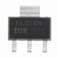
... SOT-223 Package Outline SOT-223 Part Marking Information TIO www.irf.com IRFL014N ...

Page 8

... IRFL014N SOT-223 Tape & Reel Information (. (. (. (. & 330.0 0 (13.000 LIN WORLD HEADQUARTERS: 233 Kansas St., El Segundo, California 90245, Tel: (310) 252-7105 IR GREAT BRITAIN: Hurst Green, Oxted, Surrey RH8 9BB, UK Tel 1883 732020 IR JAPAN: K&H Bldg., 2F, 30-4 Nishi-Ikebukuro 3-Chome, Toshima-Ku, Tokyo Japan 171 Tel 3983 0086 IR SOUTHEAST ASIA: 1 Kim Seng Promenade, Great World City West Tower, 13-11, Singapore 237994 Tel 838 4630 IR TAIWAN:16 Fl ...

Related keywords