IXTK250N10 IXYS, IXTK250N10 Datasheet
Home Discrete Semiconductor Products MOSFETs, GaNFETs - Single IXTK250N10
Manufacturer Part Number
IXTK250N10
Description
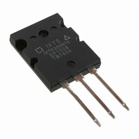
MOSFET N-CH 100V 250A TO-264AA
Specifications of IXTK250N10
Fet Type
MOSFET N-Channel, Metal Oxide
Fet Feature
Standard
Rds On (max) @ Id, Vgs
5 mOhm @ 90A, 10V
Drain To Source Voltage (vdss)
100V
Current - Continuous Drain (id) @ 25° C
250A
Vgs(th) (max) @ Id
4V @ 250µA
Gate Charge (qg) @ Vgs
430nC @ 10V
Input Capacitance (ciss) @ Vds
12700pF @ 25V
Power - Max
730W
Mounting Type
Through Hole
Package / Case
TO-264AA
Configuration
Single
Transistor Polarity
N-Channel
Resistance Drain-source Rds (on)
0.005 Ohms
Drain-source Breakdown Voltage
100 V
Gate-source Breakdown Voltage
+/- 20 V
Continuous Drain Current
250 A
Power Dissipation
730 W
Maximum Operating Temperature
+ 150 C
Mounting Style
Through Hole
Minimum Operating Temperature
- 55 C
Vdss, Max, (v)
100
Id(cont), Tc=25°c, (a)
250
Rds(on), Max, Tj=25°c, (?)
0.005
Ciss, Typ, (pf)
7800
Qg, Typ, (nc)
390
Trr, Typ, (ns)
150
Pd, (w)
730
Rthjc, Max, (k/w)
0.17
Package Style
TO-264
Lead Free Status / RoHS Status
Lead free / RoHS Compliant
Available stocks
© 2004 IXYS All rights reserved
High Current
MegaMOS
N-Channel Enhancement Mode
Symbol
V
V
V
V
I
I
I
I
E
E
dv/dt
P
T
T
T
T
M
Weight
Symbol
(T
V
V
I
I
R
D25
D(RMS)
DM
AR
GSS
DSS
J
JM
stg
L
DGR
GS
GSM
AR
D
GS(th)
DSS
AS
DSS
DS(on)
d
J
= 25°C unless otherwise specified)
T
1.6 mm (0.063 in.) from case for 10 s
Mounting torque
TO-264
Test conditions
T
T
Continuous
Transient
T
External lead current limit
T
T
I
T
Test Conditions
V
V
V
V
V
V
Pulse test, t ≤ 300 ms, duty cycle d ≤ 2%
T
T
S
C
J
J
C
C
C
J
GS
GS
GS
C
C
DS
GS
DS
= 25°C to 150°C
= 25°C to 150°C; R
= 25°C MOSFET chip capability
= 25°C, pulse width limited by T
= 25°C
= 25°C
= 25°C
≤ I
≤ 150°C, R
= 25°C
= 0 V, I
= V
= ±20 V DC, V
= V
= 0 V
= 10 V, I
DM
GS
DSS
, di/dt ≤ 100 A/µs, V
, I
TM
D
D
= 1 mA
D
= 250 µA
= 90 A
G
FET
= 2 Ω
DS
= 0
GS
= 1.0 MΩ
DD
≤ V
T
T
J
J
= 125°C
= 25°C
DSS
JM
100
IXTK 250N10
Min. Typ.
2.0
Characteristic Values
-55 ... +150
-55 ... +150
Maximum ratings
1000
0.7/6
±20
±30
100
100
250
730
150
300
4.0
75
90
80
10
5
±200
4.0
50
Nm/lb.in.
Max.
1 mA
5 mΩ
V/ns
mJ
° C
° C
° C
° C
nA
µA
W
V
A
A
A
A
V
g
J
V
V
V
V
TO-264 AA (IXTK)
G = Gate
S = Source
Features
•
•
•
•
Applications
•
•
•
•
•
Advantages
•
•
•
V
I
R
Low R
Rugged polysilicon gate cell structure
International standard package
Fast switching times
DC-DC Converters
Linear Regulators
Motor controls
DC choppers
Switched-mode power supplies
Easy to mount with one screw
(isolated mounting screw hole)
Space savings
High power density
D25
DSS
DS(on)
G
DS (on)
D
S
HDMOS
= 100
= 250
=
D
Tab = Drain
= Drain
TM
DS99022A(04/04)
5 mΩ Ω Ω Ω Ω
process
A
V
D (TAB)
Related parts for IXTK250N10
IXTK250N10 Summary of contents
... ± GSS DSS DS DSS DS(on Pulse test, t ≤ 300 ms, duty cycle d ≤ 2% © 2004 IXYS All rights reserved IXTK 250N10 Maximum ratings 100 = 1.0 MΩ 100 ±20 ±30 250 75 1000 4.0 ≤ DSS 730 -55 ... +150 150 -55 ... +150 300 0.7/6 10 Characteristic Values Min ...
... GS Pulse test, t ≤ 300 µs, duty cycle d ≤ 30A, -di/dt = 100 A/µ IXYS reserves the right to change limits, test conditions, and dimensions. IXYS MOSFETs and IGBTs are covered by one or more of the following U.S. patents: Characteristic values Min. Typ. Max. 75 110 12700 ...
... V - Volts D S Fig. 5. Drain Current vs. Case Tem perature 270 240 210 180 150 120 -50 - Degrees Centigrade C © 2004 IXYS All rights reserved º C 360 320 280 240 200 7V 160 120 1.2 1.4 1.6 º C 1.8 1.6 7V 1.4 6V 1.2 0 ...
... Safe Operating Area 10000 R Limit DS(on) 1000 100 Volts D S IXYS reserves the right to change limits, test conditions, and dimensions. IXYS MOSFETs and IGBTs are covered by one or more of the following U.S. patents: 330 300 270 240 210 180 150 120 100000 10000 1000 ...
Related keywords
ixtk200n10p ixtk250n10 IXTK250N10 datasheet IXTK250N10 data sheet IXTK250N10 pdf datasheet IXTK250N10 component IXTK250N10 part IXTK250N10 distributor IXTK250N10 RoHS IXTK250N10 datasheet download