IRF6611TR1PBF International Rectifier, IRF6611TR1PBF Datasheet

MOSFET N-CH 30V 32A DIRECTFET

IRF6611TR1PBF

Manufacturer Part Number
IRF6611TR1PBF
Description
MOSFET N-CH 30V 32A DIRECTFET
Manufacturer
International Rectifier
Series
HEXFET®r
Datasheet

Specifications of IRF6611TR1PBF

Fet Type
MOSFET N-Channel, Metal Oxide
Fet Feature
Logic Level Gate
Rds On (max) @ Id, Vgs
2.6 mOhm @ 27A, 10V
Drain To Source Voltage (vdss)
30V
Current - Continuous Drain (id) @ 25° C
32A
Vgs(th) (max) @ Id
2.25V @ 250µA
Gate Charge (qg) @ Vgs
56nC @ 4.5V
Input Capacitance (ciss) @ Vds
4860pF @ 15V
Power - Max
3.9W
Mounting Type
Surface Mount
Package / Case
DirectFET™ Isometric MX
Transistor Polarity
N-Channel
Resistance Drain-source Rds (on)
3.4 mOhms
Drain-source Breakdown Voltage
30 V
Gate-source Breakdown Voltage
20 V
Continuous Drain Current
27 A
Power Dissipation
89 W
Gate Charge Qg
37 nC
Lead Free Status / RoHS Status
Lead free / RoHS Compliant
Other names
IRF6611TR1PBFTR
Description
The IRF6611PbF combines the latest HEXFET® Power MOSFET Silicon technology with the advanced DirectFET
lowest on-state resistance in a package that has the footprint of a SO-8 and only 0.7 mm profile. The DirectFET package is compatible with
existing layout geometries used in power applications, PCB assembly equipment and vapor phase, infra-red or convection soldering tech-
niques. Application note AN-1035 is followed regarding the manufacturing methods and processes. The DirectFET package allows dual sided
cooling to maximize thermal transfer in power systems, improving previous best thermal resistance by 80%.
The IRF6611PbF balances industry leading on-state resistance while minimizing gate charge along with ultra low package inductance to
reduce both conduction and switching losses. The reduced losses make this product ideal for high frequency/high efficiency DC-DC convert-
ers that power high current loads such as the latest generation of microprocessors. The IRF6611PbF has been optimized for parameters that
are critical in synchronous buck converter’s SyncFET sockets.
l
l
l
l
l
l
l
l
l
Applicable DirectFET Outline and Substrate Outline (see p.7,8 for details)

ƒ
Notes:
www.irf.com
V
V
I
I
I
I
E
I
Absolute Maximum Ratings
D
D
D
DM
AR
DS
GS
AS
Lead-Free (Qualified up to 260°C Reflow)
Application Specific MOSFETs
Ideal for CPU Core DC-DC Converters
Low Conduction Losses
High Cdv/dt Immunity
Low Profile (<0.7mm)
Dual Sided Cooling Compatible 
Compatible with existing Surface Mount Techniques 
RoHs Compliant 
Click on this section to link to the appropriate technical paper.
Click on this section to link to the DirectFET Website.
Surface mounted on 1 in. square Cu board, steady state.
@ T
@ T
@ T
SQ
20
15
10
A
A
C
5
0
= 25°C
= 70°C
= 25°C
0
Fig 1. Typical On-Resistance vs. Gate Voltage
1
SX
V GS, Gate -to -Source Voltage (V)
T J = 25°C
2
3
Drain-to-Source Voltage
Gate-to-Source Voltage
Continuous Drain Current, V
Pulsed Drain Current
Single Pulse Avalanche Energy
Avalanche Current
ST
4
5
6
T J = 125°C
Ãg
7
g
I D = 27A
Parameter
8
MQ
GS
GS
GS
9
@ 10V
@ 10V
@ 10V
h
10
f
MX
30V max ±20V max 2.0mΩ@ 10V 2.6mΩ@ 4.5V
Q
37nC
T
Repetitive rating; pulse width limited by max. junction temperature.
Starting T
V
C
g tot
DSS
measured with thermocouple mounted to top (Drain) of part.
6.0
5.0
4.0
3.0
2.0
1.0
0.0
MT

J
0
Fig 2. Typical On-Resistance vs. Gate Voltage
= 25°C, L = 0.91mH, R
12nC
Q
I D = 22A
gd
V
MX
GS
DirectFET™ Power MOSFET ‚
IRF6611TRPbF
10
Q G Total Gate Charge (nC)
3.3nC
Q
gs2
V DS = 24V
V DS = 15V
IRF6611PbF
Max.
20
150
220
310
±20
30
32
26
22
R
DS(on)
G
16nC
Q
= 25Ω, I
rr
TM
30
DirectFET™ ISOMETRIC
packaging to achieve the
AS
23nC
Q
= 22A.
oss
40
R
DS(on)
Units
V
1.7V
mJ
05/29/06
V
A
A
gs(th)
50
1

Related parts for IRF6611TR1PBF

IRF6611TR1PBF Summary of contents

Page 1

RoHs Compliant  l Lead-Free (Qualified up to 260°C Reflow) l Application Specific MOSFETs l Ideal for CPU Core DC-DC Converters l Low Conduction Losses l High Cdv/dt Immunity l Low Profile (<0.7mm) l Dual Sided Cooling Compatible  l ...

Page 2

Static @ T = 25°C (unless otherwise specified) J Parameter BV Drain-to-Source Breakdown Voltage DSS ∆ΒV /∆T Breakdown Voltage Temp. Coefficient DSS J R Static Drain-to-Source On-Resistance DS(on) V Gate Threshold Voltage GS(th) ∆V /∆T Gate Threshold Voltage Coefficient GS(th) ...

Page 3

Absolute Maximum Ratings Power Dissipation 25° 70°C Power Dissipation 25°C Power Dissipation D C Peak Soldering Temperature Operating Junction and J T Storage Temperature ...

Page 4

PULSE WIDTH Tj = 25° Drain-to-Source Voltage (V) Fig 4. Typical Output Characteristics 1000 15V ≤ 60µs PULSE WIDTH 100 25°C ...

Page 5

150° 25° 40°C 0 0.0 0.5 1.0 1 Source-to-Drain Voltage (V) Fig 10. Typical Source-Drain Diode Forward Voltage 160 Limited by package 140 120 ...

Page 6

Current Regulator Same Type as D.U.T. 50KΩ .2µF 12V .3µ 3mA I G Current Sampling Resistors Fig 15a. Gate Charge Test Circuit D.U 20V 0.01 Ω Fig 16a. ...

Page 7

D.U.T + ƒ • • - • + ‚ -  R • • • SD • Fig 18. DirectFET™ Substrate and PCB Layout, MX Outline ƒ (Medium Size Can, X-Designation). Please see DirectFET application note AN-1035 for all details ...

Page 8

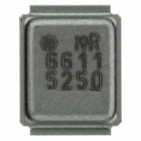
DirectFET™ Outline Dimension, MX Outline (Medium Size Can, X-Designation). Please see DirectFET application note AN-1035 for all details regarding the assembly of DirectFET. This includes all recommendations for stencil and substrate designs. DirectFET™ Part Marking 8 DIMENSIONS METRIC IMPERIAL CODE ...

Page 9

... IR WORLD HEADQUARTERS: 233 Kansas St., El Segundo, California 90245, USA Tel: (310) 252-7105 www.irf.com NOTE: Controlling dimensions in mm Std reel quantity is 4800 parts. (ordered as IRF6611TRPBF). For 1000 parts on 7" reel, order IRF6611TR1PBF REEL DIMENSIONS STANDARD OPTION (QTY 4800) TR1 OPTION (QTY 1000) ...

Page 10

Note: For the most current drawings please refer to the IR website at: http://www.irf.com/package/ ...

Related keywords