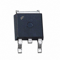
FDD8882 Fairchild Semiconductor, FDD8882 Datasheet

FDD8882
Specifications of FDD8882
Available stocks
Related parts for FDD8882
FDD8882 Summary of contents
Page 1
... D-PAK TO-252 (TO-252) ©2008 Fairchild Semiconductor Corporation FDD8882/FDU8882 Rev. C ® MOSFET General Description This N-Channel MOSFET has been designed specifically to improve the overall efficiency of DC/DC converters using either synchronous or conventional switching PWM controllers. It has been optimized for low gate charge, low r and fast switching speed ...
Page 2
... Off Characteristics B Drain to Source Breakdown Voltage VDSS I Zero Gate Voltage Drain Current DSS I Gate to Source Leakage Current GSS On Characteristics V Gate to Source Threshold Voltage GS(TH) r Drain to Source On Resistance DS(ON) FDD8882/FDU8882 Rev 25°C unless otherwise noted C Parameter 10V) (Note 4.5V) (Note 10V, with C/W) ...
Page 3
... Turn-Off Delay Time d(OFF) t Fall Time f t Turn-Off Time OFF Drain-Source Diode Characteristics V Source to Drain Diode Voltage SD t Reverse Recovery Time rr Q Reverse Recovered Charge RR Notes: 1: Package current limitation is 35A. 2: Starting T = 25° 0.1mH 28A FDD8882/FDU8882 Rev 15V 0V 1MHz V = 0.5V 1MHz 10V 10V) GS ...
Page 4
... SINGLE PULSE 0. Figure 3. Normalized Maximum Transient Thermal Impedance 600 TRANSCONDUCTANCE MAY LIMIT CURRENT IN THIS REGION V = 4.5V GS 100 FDD8882/FDU8882 Rev 25°C unless otherwise noted 150 175 125 Figure 2. Maximum Continuous Drain Current RECTANGULAR PULSE DURATION ( PULSE WIDTH (s) Figure 4 ...
Page 5
... Figure 7. Transfer Characteristics 20 PULSE DURATION = 80 s DUTY CYCLE = 0.5% MAX I = 35A GATE TO SOURCE VOLTAGE (V) GS Figure 9. Drain to Source On Resistance vs Gate Voltage and Drain Current FDD8882/FDU8882 Rev 25°C unless otherwise noted C 500 100 100 s 10 1ms 10ms DC 1 0.001 60 NOTE: Refer to Fairchild Application Notes AN7514 and AN7515 Figure 6 ...
Page 6
... T , JUNCTION TEMPERATURE ( J Figure 11. Normalized Gate Threshold Voltage vs Junction Temperature 3000 1000 C C RSS 0V 1MHz GS 100 0 DRAIN TO SOURCE VOLTAGE (V) DS Figure 13. Capacitance vs Drain to Source Voltage FDD8882/FDU8882 Rev 25°C unless otherwise noted C 1. 250 1.05 1.00 0.95 0.90 80 120 160 200 - Figure 12. Normalized Drain to Source ...
Page 7
... Test Circuits and Waveforms VARY t TO OBTAIN P R REQUIRED PEAK Figure 15. Unclamped Energy Test Circuit g(REF) Figure 17. Gate Charge Test Circuit Figure 19. Switching Time Test Circuit FDD8882/FDU8882 Rev DUT I AS 0.01 0 Figure 16. Unclamped Energy Waveforms gs2 DD - DUT g(REF) 0 Figure 18. Gate Charge Waveforms ...
Page 8
... The area, in square inches or square centimeters is the top copper area including the gate and source pads. 23.84 33.32 + ------------------------------------ - 0.268 + Area 154 33.32 + --------------------------------- - 1.73 + Area FDD8882/FDU8882 Rev and the JM 125 , application’s ambient 100 never exceeded (EQ 0.01 (0.0645 Figure 21 ...
Page 9
... PSPICE Electrical Model .SUBCKT FDD8882 rev October 2004 9e- 9e-10 Cin 6 8 1.55e-9 Dbody 7 5 DbodyMOD Dbreak 5 11 DbreakMOD Dplcap 10 5 DplcapMOD Ebreak 34.1 Eds Egs Esg Evthres Evtemp GATE Lgate 1 9 8.6e-9 Ldrain 2 5 1.0e-9 Lsource 3 7 2.67e-9 RLgate RLdrain RLsource 3 7 26.7 ...
Page 10
... FDD8882/FDU8882 Rev. C DPLCAP 10 RSLC2 - 6 ESG 8 EVTHRES + + ...
Page 11
... RTHERM1 TH 6 5.3e-2 RTHERM2 6 5 2.2e-1 RTHERM3 5 4 2.9e-1 RTHERM4 4 3 3.9e-1 RTHERM5 3 2 6.0e-1 RTHERM6 2 TL 6.6e-1 SABER Thermal Model SABER thermal model FDD8882T template thermal_model th tl thermal_c th ctherm.ctherm1 th 6 =5.6e-4 ctherm.ctherm2 6 5 =6.8e-4 ctherm.ctherm3 5 4 =2.0e-3 ctherm.ctherm4 4 3 =2.8e-3 ctherm ...
Page 12
... Definition of Terms Datasheet Identification Product Status Advance Information Formative or In Design Preliminary First Production No Identification Needed Full Production Obsolete Not In Production FDD8882/FDU8882 Rev. C FPS™ PDP-SPM™ F-PFS™ Power-SPM™ ® FRFET PowerTrench Global Power Resource SM Programmable Active Droop™ ...


