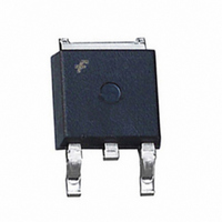
FDD120AN15A0 Fairchild Semiconductor, FDD120AN15A0 Datasheet

FDD120AN15A0
Specifications of FDD120AN15A0
Available stocks
Related parts for FDD120AN15A0
FDD120AN15A0 Summary of contents
Page 1
... GATE TO-252AA FDD SERIES T = 25°C unless otherwise noted C Parameter 10V 10V 10V) with C copper pad area certification. September 2002 DRAIN D (FLANGE Ratings Units 150 9.7 A 2.8 A Figure 4 A 122 0. -55 to 175 C o 2.31 C/W o 100 C C C/W FDP120AN15A0 / FDD120AN15A0 Rev ...
Page 2
... 10V 4A, dI /dt = 100A 4A, dI /dt = 100A Tape Width Quantity 16mm 2500 units N/A 50 units Min Typ Max 150 - - - - 150 250 100 0.101 0.120 - 0.113 0.170 - 0.235 0.282 - 770 - - 11.2 14.5 - 1.4 1.8 = 75V 3 1.0mA - 109 FDP120AN15A0 / FDD120AN15A0 Rev. B Units ...
Page 3
... Figure 2. Maximum Continuous Drain Current RECTANGULAR PULSE DURATION ( PULSE WIDTH (s) Figure 4. Peak Current Capability 50 75 100 125 150 CASE TEMPERATURE ( C) C Case Temperature NOTES: DUTY FACTOR PEAK FOR TEMPERATURES o ABOVE 25 C DERATE PEAK CURRENT AS FOLLOWS: 175 - 150 - FDP120AN15A0 / FDD120AN15A0 Rev. B 175 ...
Page 4
... DUTY CYCLE = 0.5% MAX 2.0 1.5 1.0 0.5 - Figure 10. Normalized Drain to Source On Resistance vs Junction Temperature )/(1.3*RATED DSS DD 0 *R)/(1.3*RATED +1] AS DSS DD STARTING STARTING T = 150 TIME IN AVALANCHE (ms) AV Capability V = 10V DRAIN TO SOURCE VOLTAGE ( 10V - 120 160 JUNCTION TEMPERATURE ( C) J FDP120AN15A0 / FDD120AN15A0 Rev 200 ...
Page 5
... C) Figure 12. Normalized Drain to Source Breakdown Voltage vs Junction Temperature ISS 150 Figure 14. Gate Charge Waveforms for Constant = 250 A - 120 160 JUNCTION TEMPERATURE ( 75V DD WAVEFORMS IN DESCENDING ORDER 14A GATE CHARGE (nC) g Gate Currents FDP120AN15A0 / FDD120AN15A0 Rev. B 200 12 ...
Page 6
... Figure 19. Switching Time Test Circuit ©2002 Fairchild Semiconductor Corporation DUT 0.01 Figure 16. Unclamped Energy Waveforms gs2 DUT g(REF) 0 Figure 18. Gate Charge Waveforms d(ON 90 DUT V GS 50% 10% 0 Figure 20. Switching Time Waveforms BV DSS g(TOT g(TH OFF t d(OFF 10% 10% 90% 50% PULSE WIDTH FDP120AN15A0 / FDD120AN15A0 Rev 10V 90% ...
Page 7
... C/ never exceeded (EQ 0.01 (0.0645 Figure 21. Thermal Resistance vs Mounting dissipation. Pulse (EQ. 2) Area in Inches Squared (EQ. 3) Area in Centimeters Squared R = 33.32+ 23.84/(0.268+Area) EQ 33.32+ 154/(1.73+Area) EQ (0.645) (6.45) (64. AREA, TOP COPPER AREA in (cm ) Pad Area FDP120AN15A0 / FDD120AN15A0 Rev. B ...
Page 8
... PSPICE Electrical Model .SUBCKT FDD120AN15A0 2.5e- 2.5e-10 Cin 6 8 7.5e-10 Dbody 7 5 DbodyMOD Dbreak 5 11 DbreakMOD Dplcap 10 5 DplcapMOD Ebreak 162 Eds Egs Esg Evthres Evtemp GATE Lgate 1 9 3e-9 Ldrain 2 5 1.0e-9 Lsource 3 7 2e-9 RLgate RLdrain RLsource Mmed MmedMOD ...
Page 9
... DPLCAP 10 RSLC2 - 6 ESG 8 EVTHRES + + 19 LGATE EVTEMP 8 RGATE + RLGATE CIN S1A S2A S1B S2B EGS EDS LDRAIN 5 RLDRAIN RSLC1 51 ISCL DBREAK 50 RDRAIN 11 DBODY MWEAK EBREAK MMED + MSTRO 17 18 LSOURCE - 8 7 RSOURCE RLSOURCE RBREAK 17 18 RVTEMP VBAT RVTHRES FDP120AN15A0 / FDD120AN15A0 Rev. B DRAIN 2 SOURCE 3 ...
Page 10
... Fairchild Semiconductor Corporation JUNCTION th RTHERM1 CTHERM1 6 RTHERM2 CTHERM2 5 RTHERM3 CTHERM3 4 RTHERM4 CTHERM4 3 RTHERM5 CTHERM5 2 RTHERM6 CTHERM6 tl CASE FDP120AN15A0 / FDD120AN15A0 Rev. B ...
Page 11
... TRADEMARKS The following are registered and unregistered trademarks Fairchild Semiconductor owns or is authorized to use and is not intended exhaustive list of all such trademarks. ACEx™ FACT™ ActiveArray™ FACT Quiet Series™ ® Bottomless™ FAST CoolFET™ FASTr™ CROSSVOLT™ ...


