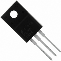
FCPF7N60 Fairchild Semiconductor, FCPF7N60 Datasheet

FCPF7N60
Specifications of FCPF7N60
FCPF7N60_NL
Available stocks
Related parts for FCPF7N60
FCPF7N60 Summary of contents
Page 1
... R Thermal Resistance, Junction-to-Case θJC R Thermal Resistance, Junction-to-Ambient θJA ©2008 Fairchild Semiconductor Corporation FCP7N60/FCPF7N60/FCPF7N60YDTU Rev. A1 Description TM SuperFET voltage MOSFET family that is utilizing an advanced charge balance mechanism for outstanding low on-resistance and lower gate charge performance. This advanced technology has been tailored to minimize con- duction loss, provide superior switching performance, and with- stand extreme dv/dt rate and higher avalanche energy ...
Page 2
... Repetitive Rating: Pulse width limited by maximum junction temperature 3.5A 50V 25Ω, Starting ≤ 7A, di/dt ≤ 200A/μs, V ≤ Starting DSS 4. Essentially Independent of Operating Temperature Typical Characteristics FCP7N60/FCPF7N60/FCPF7N60YDTU Rev. A1 Package Reel Size TO-220 TO-220F TO-220F (Forming 25°C unless otherwise noted C Conditions 250μ 0V 250μ ...
Page 3
... I , Drain Current [A] D Figure 5. Capacitance Characteristics 3000 2000 C oss C 1000 iss C rss Drain-Source Voltage [V] DS FCP7N60/FCPF7N60/FCPF7N60YDTU Rev. A1 Figure 2. Transfer Characteristics ※ Notes : 1. 250μ s Pulse Test = 25 ℃ Figure 4. Body Diode Forward Voltage 10V 20V GS ※ ℃ ...
Page 4
... J 3. Single Pulse - Drain-Source Voltage [V] DS Figure 10. Maximum Drain Current vs. Case Temperature 10.0 7.5 5.0 2.5 0 Case Temperature [ ] C FCP7N60/FCPF7N60/FCPF7N60YDTU Rev. A1 (Continued) Figure 8. On-Resistance Variation 3.0 2.5 2.0 1.5 1.0 ※ Notes : 250 μ 0.5 0.0 100 150 200 -100 o C] Figure 9-2. Maximum Safe Operating Area ...
Page 5
... Typical Performance Characteristics Figure 11-1. Transient Thermal Response Curve for FCP7N60 Figure 11-2. Transient Thermal Response Curve for FCPF7N60 FCP7N60/FCPF7N60/FCPF7N60YDTU Rev. A1 (Continued tio tio ※ ℃ ( θ (t) θ ※ ℃ ( θ (t) θ www.fairchildsemi.com ...
Page 6
... K Ω Ω Unclamped Inductive Switching Test Circuit & Waveforms FCP7N60/FCPF7N60/FCPF7N60YDTU Rev. A1 Gate Charge Test Circuit & Waveform Resistive Switching Test Circuit & Waveforms www.fairchildsemi.com ...
Page 7
... FCP7N60/FCPF7N60/FCPF7N60YDTU Rev. A1 Peak Diode Recovery dv/dt Test Circuit & Waveforms + + • • • I • www.fairchildsemi.com ...
Page 8
... Mechanical Dimensions FCP7N60/FCPF7N60/FCPF7N60YDTU Rev 220 8 Dimensions in Millimeters www.fairchildsemi.com ...
Page 9
... Mechanical Dimensions MAX1.47 0.80 ±0.10 0.35 ±0.10 2.54TYP [2.54 ] ±0.20 FCP7N60/FCPF7N60/FCPF7N60YDTU Rev. A1 (Continued) TO-220F 10.16 ø3.18 ±0.20 ±0.10 (7.00) (1.00x45°) #1 2.54TYP [2.54 ] ±0.20 9.40 ±0.20 9 2.54 ±0.20 (0.70) +0.10 0.50 2.76 ±0.20 –0.05 Dimensions in Millimeters www.fairchildsemi.com ...
Page 10
... Mechanical Dimensions FCP7N60/FCPF7N60/FCPF7N60YDTU Rev. A1 (Continued) TO-220F (Y Forming) 10 www.fairchildsemi.com ...
Page 11
... Definition of Terms Datasheet Identification Product Status Advance Information Formative / In Design Preliminary First Production No Identification Needed Full Production Obsolete Not In Production FCP7N60/FCPF7N60/FCPF7N60YDTU Rev. A1 ® FRFET Programmable Active Droop™ SM ® Global Power Resource QFET Green FPS™ QS™ Green FPS™ e-Series™ ...


