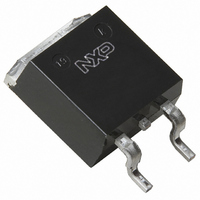
PSMN015-100B,118 NXP Semiconductors, PSMN015-100B,118 Datasheet

PSMN015-100B,118
Specifications of PSMN015-100B,118
Related parts for PSMN015-100B,118
PSMN015-100B,118 Summary of contents
Page 1
... It is not possible to make connection to pin 2 of the SOT404 package. PSMN015-100P/100B N-channel TrenchMOS™ Standard level FET Rev. 05 — 14 January 2004 Low on-state resistance DC-to-DC converters V 100 300 W tot Simplified outline ...
Page 2
... 175 100 pulsed Figure pulsed unclamped inductive load 0.11 ms starting T GS Rev. 05 — 14 January 2004 PSMN015-100P/100B N-channel TrenchMOS™ Standard level FET Min - = Figure 2 and 3 - Figure Figure © Koninklijke Philips Electronics N.V. 2004. All rights reserved. Version SOT404 Max Unit ...
Page 3
... Fig 3. Safe operating area; continuous and peak drain currents as a function of drain-source voltage. 9397 750 12543 Product data 03aa16 120 I der (%) 80 40 150 200 der Fig 2. Normalized continuous drain current Rev. 05 — 14 January 2004 PSMN015-100P/100B N-channel TrenchMOS™ Standard level FET 100 150 ------------------- = 100 function of mounting base temperature 100 ...
Page 4
... Fig 4. Transient thermal impedance from junction to mounting base as a function of pulse duration. 9397 750 12543 Product data Conditions Figure 4 vertical in still air mounted on a printed-circuit board; minimum footprint; vertical in still air Rev. 05 — 14 January 2004 PSMN015-100P/100B N-channel TrenchMOS™ Standard level FET Min Typ Max Unit - - - (s) © ...
Page 5
... Source-drain diode V source-drain (diode forward) voltage reverse recovery time rr Q recovered charge r 9397 750 12543 Product data PSMN015-100P/100B N-channel TrenchMOS™ Standard level FET Conditions I = 250 mA Figure ...
Page 6
... 4.8 V 4 4 (V) Fig 6. Transfer characteristics: drain current as a 03am55 5.2 V 5 (A) Fig 8. Normalized drain-source on-state resistance Rev. 05 — 14 January 2004 PSMN015-100P/100B N-channel TrenchMOS™ Standard level FET > DSon 175 and 175 DSon function of gate-source voltage; typical values. ...
Page 7
... Product data 03aa32 ( 120 180 Fig 10. Sub-threshold drain current as a function (pF Rev. 05 — 14 January 2004 PSMN015-100P/100B N-channel TrenchMOS™ Standard level FET min typ max ( gate-source voltage. 03am58 C iss C oss C rss (V) © Koninklijke Philips Electronics N.V. 2004. All rights reserved. 03aa35 ...
Page 8
... Product data N-channel TrenchMOS™ Standard level FET 03am57 ( 0 Fig 13. Gate-source voltage as a function of gate charge; typical values. Rev. 05 — 14 January 2004 PSMN015-100P/100B (nC and © Koninklijke Philips Electronics N.V. 2004. All rights reserved. 03am59 100 ...
Page 9
... 0.7 15.8 6.4 10.3 2.54 0.4 15.2 5.9 9.7 REFERENCES JEDEC EIAJ 3-lead TO-220AB SC-46 Rev. 05 — 14 January 2004 PSMN015-100P/100B N-channel TrenchMOS™ Standard level FET mounting base ( max. 15.0 3.30 3.8 3.0 3.0 13.5 2.79 3.6 2.7 EUROPEAN PROJECTION © ...
Page 10
... L p max. 1.60 10.30 2.90 15.80 11 2.54 1.20 9.70 2.10 14.80 REFERENCES JEDEC EIAJ Rev. 05 — 14 January 2004 PSMN015-100P/100B N-channel TrenchMOS™ Standard level FET 2 -PAK); 3 leads mounting base 2.60 2.20 EUROPEAN PROJECTION © Koninklijke Philips Electronics N.V. 2004. All rights reserved. ...
Page 11
... Philips Semiconductors 8. Revision history Table 6: Revision history Rev Date CPCN Description 05 20040114 HZG463a Product data (9397 750 12543); supersedes Product specification PSMN015-100P, PSMN015-100B Rev 1.200 of June 2003 Modifications: • • • • • • • • • 9397 750 12543 ...
Page 12
... TrenchMOS — trademark of Koninklijke Philips Electronics N.V. Rev. 05 — 14 January 2004 Rev. 05 — 14 January 2004 PSMN015-100P/100B PSMN015-100P/100B N-channel TrenchMOS™ Standard level FET N-channel TrenchMOS™ Standard level FET © Koninklijke Philips Electronics N.V. 2004. All rights reserved. © Koninklijke Philips Electronics N.V. 2004. All rights reserved. ...
Page 13
... Publication thereof does not convey nor imply any license under patent- or other industrial or intellectual property rights. Date of release: 14 January 2004 Document order number: 9397 750 12543 PSMN015-100P/100B N-channel TrenchMOS™ Standard level FET ...


