APT6013B2FLLG Microsemi Power Products Group, APT6013B2FLLG Datasheet

MOSFET N-CH 600V 43A T-MAX

APT6013B2FLLG

Manufacturer Part Number
APT6013B2FLLG
Description
MOSFET N-CH 600V 43A T-MAX
Manufacturer
Microsemi Power Products Group
Series
POWER MOS 7®r
Datasheet

Specifications of APT6013B2FLLG

Fet Type
MOSFET N-Channel, Metal Oxide
Fet Feature
Standard
Rds On (max) @ Id, Vgs
130 mOhm @ 21.5A, 10V
Drain To Source Voltage (vdss)
600V
Current - Continuous Drain (id) @ 25° C
43A
Vgs(th) (max) @ Id
5V @ 2.5mA
Gate Charge (qg) @ Vgs
130nC @ 10V
Input Capacitance (ciss) @ Vds
5630pF @ 25V
Power - Max
565W
Mounting Type
Through Hole
Package / Case
T-MAX
Lead Free Status / RoHS Status
Lead free / RoHS Compliant
STATIC ELECTRICAL CHARACTERISTICS
Power MOS 7
enhancement mode power MOSFETS. Both conduction and switching
losses are addressed with Power MOS 7
and Q
along with exceptionally fast switching speeds inherent with APT's
patented metal gate structure.
• Lower Input Capacitance
• Lower Miller Capacitance
• Lower Gate Charge, Qg
MAXIMUM RATINGS
Symbol
Symbol
T
R
BV
V
V
V
J
I
V
E
E
DS(on)
I
GS(th)
,T
I
I
DSS
GSS
P
GSM
T
DSS
DM
I
AR
GS
D
AR
AS
DSS
D
STG
L
CAUTION: These Devices are Sensitive to Electrostatic Discharge. Proper Handling Procedures Should Be Followed.
g
. Power MOS 7
POWER MOS 7
Parameter
Drain-Source Voltage
Continuous Drain Current @ T
Pulsed Drain Current
Gate-Source Voltage Continuous
Gate-Source Voltage Transient
Total Power Dissipation @ T
Linear Derating Factor
Operating and Storage Junction Temperature Range
Lead Temperature: 0.063" from Case for 10 Sec.
Avalanche Current
Repetitive Avalanche Energy
Single Pulse Avalanche Energy
Characteristic / Test Conditions
Drain-Source Breakdown Voltage (V
Drain-Source On-State Resistance
Zero Gate Voltage Drain Current (V
Gate-Source Leakage Current (V
Gate Threshold Voltage (V
®
is a new generation of low loss, high voltage, N-Channel
®
combines lower conduction and switching losses
1
1
(Repetitive and Non-Repetitive)
• Increased Power Dissipation
• Popular
• Easier To Drive
DS
C
FAST RECOVERY BODY DIODE
APT Website - http://www.advancedpower.com
= V
C
= 25°C
1
= 25°C
4
GS
GS
2
DS
, I
DS
®
= ±30V, V
GS
D
by significantly lowering R
(V
= 480V, V
= 600V, V
T-MAX™
R
= 2.5mA)
= 0V, I
GS
FREDFET
= 10V, I
DS
D
= 250µA)
GS
GS
= 0V)
or TO-264 Package
= 0V, T
= 0V)
D
= 21.5A)
All Ratings: T
C
= 125°C)
APT6013B2FLL
DS(ON)
C
600V 43A 0.130
APT6013LFLL
= 25°C unless otherwise specified.
MIN
600
B2FLL
APT6013B2LL_LLL
3
T-MAX™
-55 to 150
2500
4.52
TYP
±30
±40
600
172
565
300
43
43
50
0.130
±100
1000
MAX
250
5
TO-264
G
LFLL
Ohms
Amps
Watts
Amps
UNIT
W/°C
UNIT
Volts
Volts
Volts
Volts
mJ
°C
µA
nA
Ω Ω Ω Ω Ω
D
S

Related parts for APT6013B2FLLG

APT6013B2FLLG Summary of contents

Page 1

POWER MOS 7 ® Power MOS new generation of low loss, high voltage, N-Channel enhancement mode power MOSFETS. Both conduction and switching losses are addressed with Power MOS 7 ® and Q . Power MOS 7 combines ...

Page 2

DYNAMIC CHARACTERISTICS Symbol Characteristic C Input Capacitance iss C Output Capacitance oss C Reverse Transfer Capacitance rss Q 3 Total Gate Charge g Q Gate-Source Charge gs Q Gate-Drain ("Miller") Charge gd t Turn-on Delay Time d(on) t Rise Time ...

Page 3

RC MODEL Junction temp. (°C) 0.014 Power 0.076 (watts) 0.13 Case temperature. (°C) FIGURE 2, TRANSIENT THERMAL IMPEDANCE MODEL 160 V DS > (ON (ON)MAX. 140 250 µSEC. PULSE TEST @ <0.5 % DUTY CYCLE ...

Page 4

OPERATION HERE LIMITED (ON) 100 =+25° =+150°C SINGLE PULSE 100 V , DRAIN-TO-SOURCE VOLTAGE (VOLTS) DS FIGURE 10, MAXIMUM SAFE OPERATING AREA 43A D 12 ...

Page 5

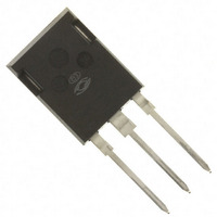
T-MAX (B2) Package Outline TM 4.69 (.185) 5.31 (.209) 1.49 (.059) 2.49 (.098) 20.80 (.819) 21.46 (.845) 4.50 (.177) Max. 0.40 (.016) 19.81 (.780) 0.79 (.031) 20.32 (.800) 2.21 (.087) 2.59 (.102) These dimensions are equal to the TO-247 without ...

Related keywords