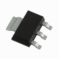
IRFL4315PBF International Rectifier, IRFL4315PBF Datasheet

IRFL4315PBF
Specifications of IRFL4315PBF
Related parts for IRFL4315PBF
IRFL4315PBF Summary of contents
Page 1
... T Operating Junction and J T Storage Temperature Range STG Soldering Temperature, for 10 seconds Thermal Resistance Symbol Parameter R Junction-to-Ambient (PCB Mount, steady state) JA Notes through † are on page 8 www.irf.com IRFL4315PbF HEXFET V R DSS mW 150V 185 Max. @ 10V GS @ 10V GS 0.02 - 150 300 (1.6mm from case ) Typ. „ ...
Page 2
... IRFL4315PbF Static @ T = 25°C (unless otherwise specified) J Parameter V Drain-to-Source Breakdown Voltage (BR)DSS Breakdown Voltage Temp. Coefficient (BR)DSS J R Static Drain-to-Source On-Resistance DS(on) V Gate Threshold Voltage GS(th) I Drain-to-Source Leakage Current DSS Gate-to-Source Forward Leakage I GSS Gate-to-Source Reverse Leakage Dynamic @ T = 25°C (unless otherwise specified) ...
Page 3
... TOP 10 BOTTOM 5.5V 5.5V 1 0.1 10 100 0.1 Fig 2. Typical Output Characteristics 2 2.0 1.5 1.0 0.5 0.0 -60 9.0 10.0 Fig 4. Normalized On-Resistance IRFL4315PbF VGS 15V 12V 10V 8.0V 7.0V 6.5V 6.0V 5.5V 20µs PULSE WIDTH Tj = 150° Drain-to-Source Voltage (V) 2. 10V GS -40 ...
Page 4
... IRFL4315PbF 10000 0V MHZ C iss = SHORTED C rss = oss = 1000 C iss 100 C oss C rss Drain-to-Source Voltage (V) Fig 5. Typical Capacitance Vs. Drain-to-Source Voltage 100 ° 150 0.1 0.0 0.5 1.0 1.5 V ,Source-to-Drain Voltage (V) SD Fig 7. Typical Source-Drain Diode Forward Voltage 1. 100 1000 Fig 6. Typical Gate Charge Vs. ...
Page 5
... RESPONSE) 0.1 0.00001 0.0001 0.001 Fig 11. Maximum Effective Transient Thermal Impedance, Junction-to-Case www.irf.com Fig 10a. Switching Time Test Circuit V DS 90% 125 150 10 d(on) Fig 10b. Switching Time Waveforms Notes: 1. Duty factor Peak T 0.01 0 Rectangular Pulse Duration (sec) 1 IRFL4315PbF + - d(off thJA A 1 ...
Page 6
... IRFL4315PbF 240 220 200 180 10V 160 140 120 100 Drain Current (A) Fig 12. On-Resistance Vs. Drain Current Current Regulator Same Type as D.U.T. V 50K 12V . D.U. 3mA Current Sampling Resistors Fig 14a&b. Basic Gate Charge Test Circuit and Waveform V (BR)DSS 20V Fig 15a&b. Unclamped Inductive Test circuit ...
Page 7
... For an Automotive Qualified version of this part please see http://www.irf.com/product-info/auto/ 2. For the most current drawing please refer to IR website at http://www.irf.com/package/ www.irf.com LOT CODE PART NUMBER 314P DAT E CODE EMBLY CODE (YYWW YEAR WW = WEEK DES IGNAT ES LEAD-FREE PRODUCT (OPT IONAL) IRFL4315PbF AXXXX BOT ...
Page 8
... IRFL4315PbF 2.05 (.080) 1.95 (.077) TR FEED DIRECTION 12.10 (.475) 11.90 (.469) NOTES : 1. CONTROLLING DIMENSION: MILLIMETER. 2. OUTLINE CONFORMS TO EIA-481 & EIA-541. 3. EACH O330.00 (13.00) REEL CONTAINS 2,500 DEVICES. 13.20 (.519) 12.80 (.504) 330.00 (13.000) MAX. NOTES : 1. OUTLINE COMFORMS TO EIA-418-1. 2. CONTROLLING DIMENSION: MILLIMETER.. ...


