IRFL4105PBF International Rectifier, IRFL4105PBF Datasheet

MOSFET N-CH 55V 3.7A SOT223

IRFL4105PBF

Manufacturer Part Number
IRFL4105PBF
Description
MOSFET N-CH 55V 3.7A SOT223
Manufacturer
International Rectifier
Series
HEXFET®r
Datasheets

Specifications of IRFL4105PBF

Fet Type
MOSFET N-Channel, Metal Oxide
Fet Feature
Logic Level Gate
Rds On (max) @ Id, Vgs
45 mOhm @ 3.7A, 10V
Drain To Source Voltage (vdss)
55V
Current - Continuous Drain (id) @ 25° C
3.7A
Vgs(th) (max) @ Id
4V @ 250µA
Gate Charge (qg) @ Vgs
35nC @ 10V
Input Capacitance (ciss) @ Vds
660pF @ 25V
Power - Max
1W
Mounting Type
Surface Mount
Package / Case
SOT-223 (3 leads + Tab), SC-73, TO-261
Current, Drain
3.7 A
Gate Charge, Total
23 nC
Package Type
SOT-223
Polarization
N-Channel
Power Dissipation
1 W
Resistance, Drain To Source On
0.045 Ohm
Temperature, Operating, Maximum
+150 °C
Temperature, Operating, Minimum
-55 °C
Time, Turn-off Delay
19 ns
Time, Turn-on Delay
7.1 ns
Transconductance, Forward
3.8 S
Voltage, Breakdown, Drain To Source
55 V
Voltage, Forward, Diode
1.3 V
Voltage, Gate To Source
±20 V
Lead Free Status / RoHS Status
Lead free / RoHS Compliant
Other names
*IRFL4105PBF
Description
Fifth Generation HEXFETs from International Rectifier
utilize advanced processing techniques to achieve
extremely low on-resistance per silicon area. This benefit,
combined with the fast switching speed and ruggedized
device design that HEXFET Power MOSFETs are well
known for, provides the designer with an extremely efficient
and reliable device for use in a wide variety of applications.
The SOT-223 package is designed for surface-mount
using vapor phase, infra red, or wave soldering techniques.
Its unique package design allows for easy automatic pick-
and-place as with other SOT or SOIC packages but has the
added advantage of improved thermal performance due to
an enlarged tab for heatsinking. Power dissipation of 1.0W
is possible in a typical surface mount application.
Absolute Maximum Ratings
Thermal Resistance
* When mounted on FR-4 board using minimum recommended footprint.
** When mounted on 1 inch square copper board, for comparison with other SMD devices.
www.irf.com
I
I
I
I
P
P
V
E
I
E
dv/dt
T
R
R
D
D
D
DM
AR
J,
D
D
GS
AS
AR
θJA
θJA
@ T
@ T
@ T
Surface Mount
Advanced Process Technology
Ultra Low On-Resistance
Dynamic dv/dt Rating
Fast Switching
Fully Avalanche Rated
Lead-Free
@T
@T
T
STG
A
A
A
A
A
= 25°C
= 25°C
= 70°C
= 25°C
= 25°C
Continuous Drain Current, V
Pulsed Drain Current
Power Dissipation (PCB Mount)**
Power Dissipation (PCB Mount)*
Linear Derating Factor (PCB Mount)*
Gate-to-Source Voltage
Single Pulse Avalanche Energy
Avalanche Current
Repetitive Avalanche Energy
Peak Diode Recovery dv/dt
Junction and Storage Temperature Range
Junction-to-Amb. (PCB Mount, steady state)*
Junction-to-Amb. (PCB Mount, steady state)**
Parameter
Parameter
GS
GS
GS
@ 10V**
@ 10V*
@ 10V*
G
Typ.
90
50
IRFL4105PbF
S
D
HEXFET
-55 to + 150
SOT-223
Max.
0.10
± 20
110
5.2
3.7
3.0
2.1
1.0
8.3
5.0
3.7
30
R
®
DS(on)
Max.
Power MOSFET
V
120
60
I
DSS
D
= 3.7A
= 0.045Ω
= 55V
PD- 95319
mW/°C
Units
Units
°C/W
V/ns
mJ
mJ
°C
W
W
A
V
A
1
05/25/04

Related parts for IRFL4105PBF

IRFL4105PBF Summary of contents

Page 1

... Thermal Resistance Parameter R Junction-to-Amb. (PCB Mount, steady state)* θJA R Junction-to-Amb. (PCB Mount, steady state)** θJA * When mounted on FR-4 board using minimum recommended footprint. ** When mounted on 1 inch square copper board, for comparison with other SMD devices. www.irf.com IRFL4105PbF HEXFET 10V 10V 10V 150 Typ ...

Page 2

... IRFL4105PbF Electrical Characteristics @ T Parameter V Drain-to-Source Breakdown Voltage (BR)DSS ∆V Breakdown Voltage Temp. Coefficient /∆T (BR)DSS J R Static Drain-to-Source On-Resistance DS(on) V Gate Threshold Voltage GS(th) g Forward Transconductance fs I Drain-to-Source Leakage Current DSS Gate-to-Source Forward Leakage I GSS Gate-to-Source Reverse Leakage Q Total Gate Charge ...

Page 3

... TOP BOTTOM 4. 0.1 10 100 Fig 2. Typical Output Characteristics 150°C J 1.0 0.5 = 25V 0.0 A 6.0 6.5 7.0 -60 Fig 4. Normalized On-Resistance IRFL4105PBF VGS 15V 10V 8.0V 7.0V 6.0V 5.5V 5.0V 4.5V 20µs PULSE WIDTH T = 150° Drain-to-Source Voltage ( 150 3. -40 ...

Page 4

... IRFL4105PbF 1200 1MHz iss rss gd 1000 oss iss 800 C oss 600 400 C rss 200 Drain-to-Source Voltage (V) DS Fig 5. Typical Capacitance Vs. Drain-to-Source Voltage 100 T = 150° 25° 0.4 0.6 0.8 1 Source-to-Drain Voltage (V) SD Fig 7. Typical Source-Drain Diode Forward Voltage SHORTED ds 16 ...

Page 5

... Fig 11. Maximum Effective Transient Thermal Impedance, Junction-to-Ambient www.irf.com 10V Pulse Width ≤ 1 µs Duty Factor ≤ 0.1 % Fig 10a. Switching Time Test Circuit d(on) Fig 10b. Switching Time Waveforms 0.01 0 Rectangular Pulse Duration (sec) 1 IRFL4105PBF D.U. d(off Notes: 1. Duty factor Peak ...

Page 6

... IRFL4105PbF D.U 20V 0.01 Ω Fig 12a. Unclamped Inductive Test Circuit Fig 12b. Unclamped Inductive Waveforms 6 300 15V 250 DRIVER 200 + - V DD 150 A 100 50 V (BR)DSS Starting T , Junction Temperature (°C) Fig 12c. Maximum Avalanche Energy I TOP 1.7A 3.0A BOTTOM 3.7A = 25V ...

Page 7

... Driver same type as D.U.T. • I controlled by Duty Factor "D" SD • D.U.T. - Device Under Test Period D = P.W. Waveform SD Body Diode Forward Current di/dt Waveform DS Diode Recovery dv/dt Body Diode Forward Drop Ripple ≤ for Logic Level Devices Fig 13. For N-Channel HEXFETS IRFL4105PBF + + P.W. Period V =10V * ...

Page 8

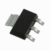
... IRFL4105PbF SOT-223 (TO-261AA) Package Outline Dimensions are shown in milimeters (inches) SOT-223 (TO-261AA) Part Marking Information HEXFET PRODUCT MARKING THIS IS AN IRFL014 INTERNATIONAL FL014 RECTIFIER LOGO TOP 8 LOT CODE PART NUMBER 314P A = ASSEMBLY SITE DATE CODE CODE (YYWW YEAR WW = WEEK P = DESIGNATES LEAD-FREE ...

Page 9

... Data and specifications subject to change without notice. Visit us at www.irf.com for sales contact information. 05/04 IRFL4105PBF 0.35 (.013) 0.25 (.010) 16.30 (.641) 15.70 (.619) 2.30 (.090) 2.10 (.083) 50.00 (1.969) MIN. ...

Related keywords