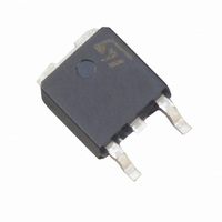
STD4NK50ZT4 STMicroelectronics, STD4NK50ZT4 Datasheet

STD4NK50ZT4
Specifications of STD4NK50ZT4
Available stocks
Related parts for STD4NK50ZT4
STD4NK50ZT4 Summary of contents
Page 1
... Such series comple- ments ST full range of high voltage MOSFETs in- cluding revolutionary MDmesh™ products. APPLICATIONS HIGH CURRENT, HIGH SPEED SWITCHING IDEAL FOR OFF-LINE POWER SUPPLIES, ADAPTORS AND PFC LIGHTING ORDERING INFORMATION SALES TYPE STP4NK50Z STP4NK50ZFP STD4NK50ZT4 STD4NK50Z-1 December 2002 STP4NK50Z - STP4NK50ZFP STD4NK50Z - STD4NK50Z ...
Page 2
STP4NK50Z - STP4NK50ZFP - STD4NK50Z - STD4NK50Z-1 ABSOLUTE MAXIMUM RATINGS Symbol Parameter V Drain-source Voltage ( Drain-gate Voltage (R DGR V Gate- source Voltage GS I Drain Current (continuous Drain Current (continuous ...
Page 3
ELECTRICAL CHARACTERISTICS (T ON/OFF Symbol Parameter V Drain-source (BR)DSS Breakdown Voltage I Zero Gate Voltage DSS Drain Current ( Gate-body Leakage GSS Current ( Gate Threshold Voltage GS(th) R Static Drain-source On DS(on) Resistance ...
Page 4
STP4NK50Z - STP4NK50ZFP - STD4NK50Z - STD4NK50Z-1 Safe Operating For TO-220 Safe Operating Area For TO-220FP Safe Operating Area For DPAK/IPAK 4/13 Thermal Impedance For TO-220 Thermal Impedance For TO-220FP Thermal Impedance For DPAK/IPAK ...
Page 5
Output Characteristics Transconductance Gate Charge vs Gate-source Voltage STP4NK50Z - STP4NK50ZFP - STD4NK50Z - STD4NK50Z-1 Transfer Characteristics Static Drain-source On Resistance Capacitance Variations 5/13 ...
Page 6
STP4NK50Z - STP4NK50ZFP - STD4NK50Z - STD4NK50Z-1 Normalized Gate Threshold Voltage vs Temp. Source-drain Diode Forward Characteristics Maximum Avalanche Energy vs Temperature 6/13 Normalized On Resistance vs Temperature Normalized BVDSS vs Temperature ...
Page 7
Fig. 1: Unclamped Inductive Load Test Circuit Fig. 3: Switching Times Test Circuit For Resistive Load Fig. 5: Test Circuit For Inductive Load Switching And Diode Recovery Times STP4NK50Z - STP4NK50ZFP - STD4NK50Z - STD4NK50Z-1 Fig. 2: Unclamped Inductive Waveform ...
Page 8
STP4NK50Z - STP4NK50ZFP - STD4NK50Z - STD4NK50Z-1 DIM. MIN. A 4.40 C 1. 0.49 F 0.61 F1 1.14 F2 1.14 G 4.95 G1 2 13.0 L5 2.65 L6 15.25 L7 6.2 L9 ...
Page 9
STP4NK50Z - STP4NK50ZFP - STD4NK50Z - STD4NK50Z-1 TO-220FP MECHANICAL DATA mm. DIM. MIN. TYP A 4.4 B 2.5 D 2.5 E 0.45 F 0.75 F1 1.15 F2 1.15 G 4. 28.6 L4 9.8 L5 ...
Page 10
STP4NK50Z - STP4NK50ZFP - STD4NK50Z - STD4NK50Z-1 DIM. MIN. A 2.20 A1 0.90 A2 0.03 B 0.64 B2 5.20 C 0.45 C2 0.48 D 6.00 E 6.40 G 4. 10/13 TO-252 (DPAK) ...
Page 11
STP4NK50Z - STP4NK50ZFP - STD4NK50Z - STD4NK50Z-1 TO-251 (IPAK) MECHANICAL DATA mm DIM. MIN. TYP. A 2.2 A1 0.9 A3 0.7 B 0. 0. 6.4 G 4.4 H ...
Page 12
STP4NK50Z - STP4NK50ZFP - STD4NK50Z - STD4NK50Z-1 DPAK FOOTPRINT All dimensions are in millimeters TAPE AND REEL SHIPMENT (suffix ”T4”)* TAPE MECHANICAL DATA mm DIM. MIN. MAX. MIN. A0 6.8 7 0.267 0.275 B0 10.4 10.6 0.409 0.417 B1 12.1 ...
Page 13
... No license is granted by implication or otherwise under any patent or patent rights of STMicroelectronics. Specifications mentioned in this publication are subject to change without notice. This publication supersedes and replaces all information previously supplied ...


