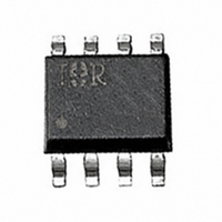
IRF7342D2PBF International Rectifier, IRF7342D2PBF Datasheet

IRF7342D2PBF
Specifications of IRF7342D2PBF
Related parts for IRF7342D2PBF
IRF7342D2PBF Summary of contents
Page 1
... Repetitive rating – pulse width limited by max. junction temperature (see fig. 11) ‚ ≤ -3.4A, di/dt ≤ -150A/µs, V ≤ ƒ Pulse width ≤ 400µs – duty cycle ≤ 2% „ Surface mounted on 1 inch square copper board, t ≤ 10sec. www.irf.com IRF7342D2PbF FETKY MOSFET & Schottky Diode Top View and = 25° ...
Page 2
... IRF7342D2PbF Electrical Characteristics @ T Parameter V Drain-to-Source Breakdown Voltage (BR)DSS Breakdown Voltage Temp. Coefficient ∆V /∆T (BR)DSS J R Static Drain-to-Source On-Resistance DS(on) V Gate Threshold Voltage GS(th) g Forward Transconductance fs I Drain-to-Source Leakage Current DSS Gate-to-Source Forward Leakage Gate-to-Source Reverse Leakage Q Total Gate Charge g Q Gate-to-Source Charge ...
Page 3
... Power Mosfet Characteristics 100 TOP 10 BOTTOM 1 0.1 0.1 10 100 2 1.5 ° 150 C J 1.0 0.5 = -25V 0.0 -60 -40 -20 6.0 7.0 IRF7342D2PbF VGS -15V -10V - 6.0V -5.5V -4.5V -3.5V -3.0V - 2.5V -2.5V 20µs PULSE WIDTH Tj = 150° Drain-to-Source Voltage (V) -3 -10V 100 120 140 160 ° ...
Page 4
... IRF7342D2PbF 1000 1MHz iss rss 800 oss iss 600 400 200 C oss C rss Drain-to-Source Voltage (V) DS Fig 5. Typical Capacitance Vs. Drain-to-Source Voltage 100 10 ° 150 0.1 0.2 0.4 0.6 0.8 -V ,Source-to-Drain Voltage (V) SD Fig 7. Typical Source-Drain Diode Forward Voltage 4 Power Mosfet Characteristics ...
Page 5
... Fig 11. Maximum Effective Transient Thermal Impedance, Junction-to-Ambient www.irf.com Power Mosfet Characteristics Fig 10a. Switching Time Test Circuit V GS 10% 125 150 ° 90 Fig 10b. Switching Time Waveforms 0.01 0 Rectangular Pulse Duration (sec) 1 IRF7342D2PbF - + ≤ 1 ≤ 0 d(on) r d(off Notes: 1. Duty factor ...
Page 6
... IRF7342D2PbF 0.25 0.20 0. -3.4A 0.10 0.05 3.0 5.0 7.0 9.0 -V GS, Gate -to -Source Voltage (V) Fig 12. Typical On-Resistance Vs. Gate Voltage Charge Fig 14a. Basic Gate Charge Waveform 6 Power Mosfet Characteristics 0.35 0.30 0.25 0.20 0.15 0.10 0.05 11.0 13.0 15.0 0.0 Fig 13. Typical On-Resistance Vs. ...
Page 7
... Temperature ( °C ) Fig 15. Typical Vgs(th) Vs. Junction Temperature www.irf.com Power Mosfet Characteristics 100 -250µ 0.001 75 100 125 150 Fig 16. Typical Power Vs. Time IRF7342D2PbF 0.010 0.100 1.000 10.000 100.000 Time (sec) 7 ...
Page 8
... IRF7342D2PbF 100 0.4 0.8 1.2 1.6 Forward Voltage Drop - V Fig Maximum Forward Voltage Drop Characteristics 8 Schottky Diode Characteristics 100 10 1 0.1 0. 150°C J 0.001 T = 125° 25°C J Reverse Current Vs. Reverse Voltage 1000 100 2 2.4 2.8 ( Fig Typical Junction Capacitance T = 150°C J 125° ...
Page 9
... Inverse Power Loss = REV R1 www.irf.com Notes: 1. Duty factor Peak 0.001 0.01 0 Rectangular Pulse Duration (sec thJA = 62.5 °C/W DC see note (4) S quare wave ( D = 0.50 Rated V R applied Average Forward Current - I F(AV) (A) Temp. Vs. Forward Current ) REV thJA / @ ( F(AV D 80% rated IRF7342D2PbF thJA 100 6 9 ...
Page 10
... IRF7342D2PbF SO-8 (Fetky) Package Outline 0.25 [.010 NOTES : 1. DIMENS IONING & TOLERANCING PER AS ME Y14.5M-1994. 2. CONTROLLING DIMENS ION: MILLIMETER 3. DIMENS IONS ARE S HOWN IN MILLIMET ERS [INCHES ]. 4. OUT LINE CONF ORMS TO JEDEC OUTLINE MS -012AA. 5 DIMENS ION DOES NOT INCLUDE MOLD PROTRUS IONS . ...
Page 11
... Data and specifications subject to change without notice. This product has been designed and qualified for the Consumer market. Qualification Standards can be found on IR’s Web site. Visit us at www.irf.com for sales contact information.10/04 IRF7342D2PbF 12.3 ( .484 ) 11.7 ( .461 ) FEED DIRECTION 14.40 ( .566 ) 12 ...


