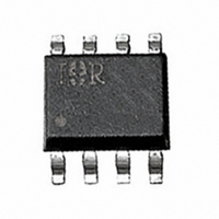
IRF7807VD2PBF International Rectifier, IRF7807VD2PBF Datasheet

IRF7807VD2PBF
Specifications of IRF7807VD2PBF
Related parts for IRF7807VD2PBF
IRF7807VD2PBF Summary of contents
Page 1
... SO-8 ® MOSFETs and DEVICE CHARACTERISTICS… Symbol 25° 70° 25° 70°C 25°C I (AV) F 70° STG R θJA R θJL PD-95291 IRF7807VD2PbF Top View IRF7807VD2 17mΩ DS (on) 9.5nC G 3.4nC sw 12nC oss Max. Units 30 V ±20 8.3 6 2.5 W 1.6 3 ...
Page 2
... IRF7807VD2PbF Electrical Characteristics Parameter Drain-to-Source BV DSS Breakdown Voltage Static Drain-Source R DS (on) on Resistance Gate Threshold Voltage V GS(th) Drain-Source Leakage I DSS Current Current* Gate-Source Leakage I GSS Current* Total Gate Charge Pre-Vth Q GS1 Gate-Source Charge Post-Vth Q GS2 Gate-Source Charge Gate to Drain Charge Q GD ...
Page 3
... P P loss conduction ( = I P loss rms ( + Q gs2 ⎛ ⎜ ⎝ , can be seen from *dissipated primarily in Q1 critical fac- gs2 is formed by the when multiplied by IRF7807VD2PbF 4 Drain Current 1 Gate Voltage Drain Voltage + drive output ) 2 × R ds(on) ) × V × ⎞ ( × V × × V × f oss ⎠ ...
Page 4
... IRF7807VD2PbF For the synchronous MOSFET Q2, R portant characteristic; however, once again the im- portance of gate charge must not be overlooked since it impacts three critical areas. Under light load the MOSFET must still be turned on and off by the con- trol IC so the gate drive losses become much more significant ...
Page 5
... BOTTOM 0. 380µs PULSE WIDTH Tj = 25° 0.2 0.4 0 Source-to-Drain Voltage (V) Fig 7. Typical Reverse Output Characteristics www.irf.com IRF7807VD2PbF 0.030 0.025 0.020 0.015 V = 4.5V GS 0.010 2.0 4.0 6.0 ° V GS, Gate -to -Source Voltage (V) Fig 7. On-Resistance Vs. Gate Voltage 70 TOP 60 50 BOTTOM 0 ...
Page 6
... IRF7807VD2PbF 100 D = 0.50 0.20 10 0.10 0.05 0.02 1 0.01 SINGLE PULSE (THERMAL RESPONSE) 0.1 0.00001 0.0001 Figure 9. Maximum Effective Transient Thermal Impedance, Junction-to-Ambient 0.001 0. Rectangular Pulse Duration (sec 7. 16V Total Gate Charge (nC) G Fig 10. Typical Gate Charge Vs. Gate-to-Source Voltage Notes: 1. Duty factor ...
Page 7
... Forward Voltage Drop - Fig Typical Forward Voltage Drop Characteristics www.irf.com 100 Tj = 150° 0.1 0.01 0.001 0 Reverse Current Vs. Reverse Voltage 0.8 1.0 1.2 IRF7807VD2PbF 125°C 100°C 75°C 50°C 25° Reverse Voltage - V R (V) Fig Typical Values ...
Page 8
... IRF7807VD2PbF SO-8 (Fetky) Package Outline 0.25 [.010 NOT DIMENS IONING & TOLERANCING PER ASME Y14.5M-1994. 2. CONT ROLLING DIMENS ION: MILLIMET ER 3. DIMENS IONS ARE SHOWN IN MILLIMETERS [INCHES]. 4. OUTLINE CONFORMS TO JEDEC OUTLINE MS -012AA. 5 DIMENS ION DOES NOT INCLUDE MOLD PROT RUSIONS . MOLD PROTRUS IONS NOT TO EXCEED 0.15 [.006]. ...
Page 9
... Data and specifications subject to change without notice. This product has been designed and qualified for the Consumer market. Qualifications Standards can be found on IR’s Web site. Visit us at www.irf.com for sales contact information.10/04 IRF7807VD2PbF 12.3 ( .484 ) 11.7 ( .461 ) 14.40 ( .566 ) 12.40 ( .488 ) ...


