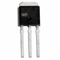
IRLU3715ZPBF International Rectifier, IRLU3715ZPBF Datasheet

IRLU3715ZPBF
Specifications of IRLU3715ZPBF
Related parts for IRLU3715ZPBF
IRLU3715ZPBF Summary of contents
Page 1
... Storage Temperature Range STG Soldering Temperature, for 10 seconds Thermal Resistance Parameter R Junction-to-Case θJC Junction-to-Ambient (PCB Mount) R θJA R Junction-to-Ambient θJA Notes through are on page 11 … www.irf.com IRLR3715ZPbF IRLU3715ZPbF HEXFET Power MOSFET V R DSS 20V IRLR3715Z Max. 20 ± 10V 10V 35 GS 200 40 20 ...
Page 2
Static @ T = 25°C (unless otherwise specified) J Parameter BV Drain-to-Source Breakdown Voltage DSS ∆ΒV /∆T Breakdown Voltage Temp. Coefficient DSS J R Static Drain-to-Source On-Resistance DS(on) V Gate Threshold Voltage GS(th) ∆V /∆T Gate Threshold Voltage Coefficient GS(th) ...
Page 3
VGS TOP 10V 4.5V 1000 3.7V 3.5V 3.3V 3.0V 100 2.7V BOTTOM 2. 0.1 20µs PULSE WIDTH Tj = 25°C 0.01 0 Drain-to-Source Voltage (V) Fig 1. Typical Output Characteristics 1000 100 10 ...
Page 4
0V MHZ C iss = SHORTED C rss = oss = 1000 C iss C oss C ...
Page 5
Limited By Package 100 Case Temperature (°C) Fig 9. Maximum Drain Current vs. Case Temperature 0.50 1 0.20 0.10 0.05 0.02 0.1 0.01 SINGLE PULSE ...
Page 6
D.U 20V V GS 0.01 Ω Fig 12a. Unclamped Inductive Test Circuit Fig 12b. Unclamped Inductive Waveforms Current Regulator Same Type as D.U.T. 50KΩ .2µF 12V ...
Page 7
D.U.T + ƒ • • - • + ‚ - R • • • SD • Fig 15. Vds Vgs(th) Qgs1 Qgs2 www.irf.com Driver Gate Drive P.W. D.U.T. I Waveform SD Reverse Recovery „ Current - + D.U.T. V ...
Page 8
Power MOSFET Selection for Non-Isolated DC/DC Converters Control FET loss conduction switching drive This can be expanded and approximated by × loss rms ds(on ) ⎛ ...
Page 9
EXAMPLE: T HIS IS AN IRFR120 WITH AS S EMBLY LOT CODE 1234 AS S EMBLED ON WW 16, 1999 IN THE AS S EMBLY LINE "A" Note: "P" sembly line pos ition indicates "Lead-Free" OR www.irf.com INTERNATIONAL ...
Page 10
EXAMPLE: T HIS IS AN IRFU120 WIT EMBLY LOT CODE 5678 AS S EMBLED ON WW 19, 1999 EMBLY LINE "A" Note: "P" in assembly line position indicates "Lead-Free" OR INT ERNAT ...
Page 11
TR 12.1 ( .476 ) 11.9 ( .469 ) NOTES : 1. CONTROLLING DIMENSION : MILLIMETER. 2. ALL DIMENSIONS ARE SHOWN IN MILLIMETERS ( INCHES ). 3. OUTLINE CONFORMS TO EIA-481 & EIA-541. 13 INCH NOTES : 1. OUTLINE CONFORMS ...
Page 12
Note: For the most current drawings please refer to the IR website at: http://www.irf.com/package/ ...


