IRFP1405PBF International Rectifier, IRFP1405PBF Datasheet

MOSFET N-CH 55V 95A TO-247AC

IRFP1405PBF

Manufacturer Part Number
IRFP1405PBF
Description
MOSFET N-CH 55V 95A TO-247AC
Manufacturer
International Rectifier
Series
HEXFET®r
Datasheets

Specifications of IRFP1405PBF

Fet Type
MOSFET N-Channel, Metal Oxide
Fet Feature
Standard
Rds On (max) @ Id, Vgs
5.3 mOhm @ 95A, 10V
Drain To Source Voltage (vdss)
55V
Current - Continuous Drain (id) @ 25° C
95A
Vgs(th) (max) @ Id
4V @ 250µA
Gate Charge (qg) @ Vgs
180nC @ 10V
Input Capacitance (ciss) @ Vds
5600pF @ 25V
Power - Max
310W
Mounting Type
Through Hole
Package / Case
TO-247-3 (Straight Leads), TO-247AC
Transistor Polarity
N Channel
Continuous Drain Current Id
160A
Drain Source Voltage Vds
55V
On Resistance Rds(on)
5.3mohm
Rds(on) Test Voltage Vgs
10V
Threshold Voltage Vgs Typ
4V
Rohs Compliant
Yes
Drain-source Breakdown Voltage
55 V
Gate-source Breakdown Voltage
20 V
Continuous Drain Current
160 A
Power Dissipation
310 W
Mounting Style
Through Hole
Gate Charge Qg
120 nC
Lead Free Status / RoHS Status
Lead free / RoHS Compliant
Other names
*IRFP1405PBF

Available stocks

Company
Part Number
Manufacturer
Quantity
Price
Part Number:
IRFP1405PBF
Manufacturer:
IR
Quantity:
8 000
Company:
Part Number:
IRFP1405PBF
Quantity:
9 000
Company:
Part Number:
IRFP1405PBF
Quantity:
5 624
Description
Features
HEXFET
*
This HEXFET
processing techniques to achieve extremely low
on-resistance per silicon area. Additional features
of this design are a 175°C junction operating
temperature, fast switching speed and improved
repetitive avalanche rating. These features
combine to make this design an extremely efficient
and reliable device for use in a wide variety of
applications.
I
I
I
I
P
V
E
E
I
E
T
T
R
R
R
www.irf.com
Absolute Maximum Ratings
Thermal Resistance
D
D
D
DM
AR
J
STG
D
GS
AS (Thermally limited)
AS
AR
JC
cs
JA
@ T
@ T
@ T
Advanced Process Technology
Ultra Low On-Resistance
175°C Operating Temperature
Fast Switching
Repetitive Avalanche Allowed up to Tjmax
Lead-Free
@T
(Tested )
C
C
C
C
= 25°C Continuous Drain Current, V
= 100°C Continuous Drain Current, V
= 25°C Continuous Drain Current, V
= 25°C Power Dissipation
®
is a registered trademark of International Rectifier.
®
Power MOSFET utilizes the latest
Pulsed Drain Current
Linear Derating Factor
Gate-to-Source Voltage
Single Pulse Avalanche Energy
Single Pulse Avalanche Energy Tested Value
Avalanche Current
Repetitive Avalanche Energy
Operating Junction and
Storage Temperature Range
Soldering Temperature, for 10 seconds
Mounting Torque, 6-32 or M3 screw
Junction-to-Case *
Case-to-Sink, Flat, Greased Surface
Junction-to-Ambient *
Ã
Parameter
Parameter
GS
GS
GS
g
@ 10V
@ 10V
@ 10V
d
(Silicon Limited)
(Package Limited)
h
G
IRFP1405PbF
Typ.
See Fig.12a, 12b, 15, 16
HEXFET
300 (1.6mm from case )
0.24
–––
–––
10 lbf
TO-247AC
D
S
-55 to + 175
y
Max.
1060
in (1.1N
160
110
640
310
± 20
530
2.0
95
®
R
Power MOSFET
DS(on)
y
V
m)
Max.
0.49
DSS
I
–––
40
D
= 95A
PD - 95509A
= 5.3m
= 55V
Units
Units
W/°C
°C/W
mJ
mJ
°C
W
A
V
A
1

Related parts for IRFP1405PBF

IRFP1405PBF Summary of contents

Page 1

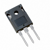
... Case-to-Sink, Flat, Greased Surface cs R Junction-to-Ambient * JA ® HEXFET is a registered trademark of International Rectifier. * www.irf.com G Parameter @ 10V (Silicon Limited 10V GS @ 10V (Package Limited Parameter PD - 95509A IRFP1405PbF ® HEXFET Power MOSFET 55V DSS R = 5.3m DS(on 95A D S TO-247AC Max. Units 160 110 95 640 310 W 2.0 W/° ...

Page 2

Electrical Characteristics @ T Parameter V Drain-to-Source Breakdown Voltage (BR)DSS Breakdown Voltage Temp. Coefficient (BR)DSS J R Static Drain-to-Source On-Resistance DS(on) V Gate Threshold Voltage GS(th) gfs Forward Transconductance I Drain-to-Source Leakage Current DSS I Gate-to-Source Forward ...

Page 3

VGS TOP 15V 10V 8.0V 7.0V 6.0V 5.5V 100 5.0V BOTTOM 4.5V 4.5V 10 60µs PULSE WIDTH Tj = 25° Drain-to-Source Voltage (V) Fig 1. Typical Output Characteristics 1000 25°C ...

Page 4

0V MHZ C iss = SHORTED C rss = C gd 8000 C oss = Ciss 6000 4000 Coss 2000 ...

Page 5

LIMITED BY PACKAGE 150 100 100 Case Temperature (°C) Fig 9. Maximum Drain Current Vs. Case Temperature 0.50 0.20 0.1 0.10 0.05 0.02 0.01 0.01 0.001 SINGLE PULSE ...

Page 6

D.U 20V Fig 12a. Unclamped Inductive Test Circuit V (BR)DSS Fig 12b. Unclamped Inductive Waveforms Charge ...

Page 7

Duty Cycle = Single Pulse 1000 0.01 100 0.05 0. 1.0E-06 1.0E-05 Fig 15. Typical Avalanche Current Vs.Pulsewidth 600 TOP Single Pulse BOTTOM 1% Duty Cycle 500 95A 400 300 200 100 0 25 ...

Page 8

D.U.T + ƒ ‚ -  SD Fig 17. Fig 18a. Switching Time Test Circuit V DS 90% 10 Fig 18b. Switching Time Waveforms 8 Driver Gate Drive P.W. D.U.T. I Waveform SD Reverse Recovery „ ...

Page 9

EXAMPLE: T HIS IS AN IRFPE30 WIT H ASSEMBLY LOT CODE 5657 ASSEMBLED ON WW 35, 2000 ASSEMBLY LINE "H" Note: "P" in assembly line position indicates "Lead-Free" TO-247AC packages are not recommended for Surface Mount Application. ...

Related keywords