IXFX30N100Q2 IXYS, IXFX30N100Q2 Datasheet
Home Discrete Semiconductor Products MOSFETs, GaNFETs - Single IXFX30N100Q2
Manufacturer Part Number
IXFX30N100Q2
Description
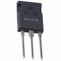
MOSFET N-CH 1000V 30A PLUS247
Specifications of IXFX30N100Q2
Fet Type
MOSFET N-Channel, Metal Oxide
Fet Feature
Standard
Rds On (max) @ Id, Vgs
400 mOhm @ 500mA, 10V
Drain To Source Voltage (vdss)
1000V (1kV)
Current - Continuous Drain (id) @ 25° C
30A
Vgs(th) (max) @ Id
5V @ 8mA
Gate Charge (qg) @ Vgs
186nC @ 10V
Input Capacitance (ciss) @ Vds
8200pF @ 25V
Power - Max
735W
Mounting Type
Through Hole
Package / Case
PLUS247™-3
Configuration
Single
Transistor Polarity
N-Channel
Resistance Drain-source Rds (on)
0.4 Ohms
Drain-source Breakdown Voltage
1000 V
Gate-source Breakdown Voltage
+/- 30 V
Continuous Drain Current
30 A
Power Dissipation
735 W
Maximum Operating Temperature
+ 150 C
Mounting Style
Through Hole
Minimum Operating Temperature
- 55 C
Vdss, Max, (v)
1000
Id(cont), Tc=25°c, (a)
30
Rds(on), Max, Tj=25°c, (?)
0.400
Ciss, Typ, (pf)
9400
Qg, Typ, (nc)
186
Trr, Typ, (ns)
-
Trr, Max, (ns)
300
Pd, (w)
735
Rthjc, Max, (ºc/w)
0.17
Package Style
PLUS247
Lead Free Status / RoHS Status
Lead free / RoHS Compliant
Available stocks
Part Number:
IXFX30N100Q2
© 2004 IXYS All rights reserved
HiPerFET
Power MOSFETs
Q-Class
Preliminary Data Sheet
Symbol
V
V
V
V
I
I
I
E
E
dv/dt
P
T
T
T
T
M
Weight
Symbol
V
V
I
I
R
N-Channel Enhancement Mode
Avalanche Rated, High dv/dt, Low Q
Low intrinsic R
D25
DM
AR
GSS
DSS
JM
L
J
stg
DSS
DGR
GS
GSM
AR
AS
D
GS(th)
DSS
DS(on)
d
Test Conditions
T
T
Continuous
Transient
T
T
T
T
T
I
T
T
1.6 mm (0.063 in) from case for 10 s
Mounting torque
Test Conditions
V
V
V
V
V
V
Pulse test, t ≤ 300 µs, duty cycle d ≤ 2 %
S
C
C
C
C
C
C
J
J
J
GS
GS
DS
DS
GS
GS
= 25°C to 150°C
= 25°C to 150°C; R
= 25°C
= 25°C, pulse width limited by T
= 25°C
= 25°C
= 25°C
≤ I
≤ 150°C, R
= 25°C
= 0 V, I
= V
= ±20 V
= V
= 0 V
= 10 V, I
g
DM
, low t
TM
, di/dt ≤ 100 A/µs, V
GS
DSS
, I
D
D
DC
D
= 3mA
= 8 mA
, V
rr
= 0.5 • I
G
= 2 Ω
DS
= 0
D25
GS
= 1 MΩ
DD
T
T
(T
J
J
≤ V
J
= 25°C
= 125°C
= 25°C, unless otherwise specified)
IXFK 30N100Q2
IXFX 30N100Q2
DSS
g
TO-264
PLUS-247
TO-264
JM
,
1000
min.
2.5
Characteristic Values
-55 ... +150
-55 ... +150
Maximum Ratings
typ.
1000
1000
0.9/6 Nm/lb.in.
150
±30
±40
120
735
300
4.0
30
30
60
20
10
6
max.
±200
0.40
5.0
50
2 mA
V/ns
mJ
µA
°C
°C
°C
°C
nA
W
Ω
V
V
V
V
A
A
A
V
V
g
g
J
PLUS 247
TO-264 AA (IXFK)
G = Gate
S = Source
Features
Advantages
Double metal process for low gate
International standard packages
classification
Avalanche energy and current rated
Fast intrinsic Rectifier
resistance
Easy to mount
Space savings
High power density
Epoxy meet UL 94 V-0, flammability
V
I
R
D25
DSS
DS(on)
G
TM
t
D
rr
(IXFX)
G
≤ ≤ ≤ ≤ ≤ 300 ns
D
= 1000 V
=
= 0.40 Ω Ω Ω Ω Ω
S
D = Drain
TAB = Drain
30 A
DS99160(4/04)
D (TAB)
D (TAB)
Related parts for IXFX30N100Q2
IXFX30N100Q2 Summary of contents
... GSS DSS DS DSS 0.5 • I DS(on D25 Pulse test, t ≤ 300 µs, duty cycle d ≤ © 2004 IXYS All rights reserved IXFK 30N100Q2 IXFX 30N100Q2 g Maximum Ratings 1000 = 1 MΩ 1000 GS ±30 ±40 30 120 4.0 ≤ DSS 735 -55 ... +150 150 -55 ... +150 ...
... Pulse test, t ≤ 300 µs, duty cycle d ≤ 25A, -di/dt = 100 A/µ IXYS reserves the right to change limits, test conditions, and dimensions. IXYS MOSFETs and IGBTs are covered by one or more of the following U.S. patents: Characteristic Values (T = 25°C, unless otherwise specified) J min. typ. , pulse test ...
... V - Volts D S Fig Norm alized to DS(on) 0.5 I Value vs. I D25 2.8 2 10V GS 2.4 2 125º 1.8 1.6 1.4 1 Amperes D © 2004 IXYS All rights reserved º 5. º C 3.1 2.8 2.5 2.2 5.5V 1.9 1.6 1.3 5V 0.7 4.5V 0 25ºC ...
... T = 125º 0.4 0.5 0.6 0.7 0 Volts S D Fig. 11. Capacitance 10000 f = 1MHz 1000 100 Volts D S IXYS reserves the right to change limits, test conditions, and dimensions. IXYS MOSFETs and IGBTs are covered by one or more of the following U.S. patents 5 25ºC ...
Related keywords
ixfx34n80 IXFX30N100Q2 datasheet IXFX30N100Q2 data sheet IXFX30N100Q2 pdf datasheet IXFX30N100Q2 component IXFX30N100Q2 part IXFX30N100Q2 distributor IXFX30N100Q2 RoHS IXFX30N100Q2 datasheet download