IXFX360N15T2 IXYS, IXFX360N15T2 Datasheet - Page 2
IXFX360N15T2
Manufacturer Part Number
IXFX360N15T2
Description
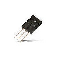
MOSFET N-CH 150V 360A PLUS247
Manufacturer
IXYS
Series
GigaMOS™r
Type
GigaMOS Trench T2 HiperFetr
Datasheet
1.IXFK360N15T2.pdf
(6 pages)
Specifications of IXFX360N15T2
Fet Type
MOSFET N-Channel, Metal Oxide
Fet Feature
Standard
Rds On (max) @ Id, Vgs
4 mOhm @ 60A, 10V
Drain To Source Voltage (vdss)
150V
Current - Continuous Drain (id) @ 25° C
360A
Vgs(th) (max) @ Id
5V @ 8mA
Gate Charge (qg) @ Vgs
715nC @ 10V
Input Capacitance (ciss) @ Vds
47500pF @ 25V
Power - Max
1670W
Mounting Type
Through Hole
Package / Case
PLUS247™-3
Product
MOSFET Gate Drivers
Rise Time
170 ns
Fall Time
265 ns
Supply Current
100 A
Maximum Power Dissipation
1670 W
Maximum Operating Temperature
+ 175 C
Mounting Style
Through Hole
Maximum Turn-off Delay Time
115 ns
Maximum Turn-on Delay Time
50 ns
Minimum Operating Temperature
- 55 C
Number Of Drivers
Single
Number Of Outputs
1
Output Current
360 A
Output Voltage
150 V
Vdss, Max, (v)
150
Id(cont), Tc=25°c, (a)
360
Rds(on), Max, Tj=25°c, (?)
0.004
Ciss, Typ, (pf)
47500
Qg, Typ, (nc)
715
Pd, (w)
1670
Rthjc, Max, (k/w)
0.09
Package Style
PLUS247
Lead Free Status / RoHS Status
Lead free / RoHS Compliant


Symbol
(T
g
C
C
C
t
t
t
t
Q
Q
Q
R
R
Source-Drain Diode
Symbol
(T
I
I
V
t
Q
I
Note 1.
IXYS Reserves the Right to Change Limits, Test Conditions, and Dimensions.
IXYS MOSFETs and IGBTs are covered
by one or more of the following U.S. patents: 4,850,072
S
SM
RM
d(on)
r
d(off)
f
rr
fs
SD
iss
oss
rss
thJC
thCS
g(on)
gs
gd
RM
J
J
The product presented herein is under development. The Technical Specifications offered are derived
from a subjective evaluation of the design, based upon prior knowledge and experience, and constitute a
"considered reflection" of the anticipated result. IXYS reserves the right to change limits, test
conditions, and dimensions without notice.
= 25°C Unless Otherwise Specified)
= 25°C, Unless Otherwise Specified)
Pulse test, t ≤ 300μs; duty cycle, d ≤ 2%.
Test Conditions
V
V
Resistive Switching Times
V
R
V
Test Conditions
V
Repetitive, Pulse Width Limited by T
I
I
V
F
F
DS
GS
GS
GS
GS
R
G
= 60A, V
= 160A, -di/dt = 100A/μs
= 60V, V
= 10V, I
= 0V, V
= 10V, V
= 1Ω (External)
= 10V, V
= 0V
ADVANCE TECHNICAL INFORMATION
GS
D
DS
GS
DS
DS
= 60A, Note 1
= 0V, Note 1
= 25V, f = 1MHz
= 0V
= 0.5 • V
= 0.5 • V
4,835,592
4,881,106
DSS
DSS
4,931,844
5,017,508
5,034,796
, I
, I
D
D
= 100A
= 0.5 • I
5,049,961
5,063,307
5,187,117
JM
D25
140
Min.
Min.
5,237,481
5,381,025
5,486,715
Characteristic Values
Characteristic Values
3060
47.5
0.15
230
665
170
115
265
715
185
200
Typ.
0.50
9.00
6,162,665
6,259,123 B1
6,306,728 B1
50
Typ.
Max.
0.09
1440
Max.
150
360
1.2
6,404,065 B1
6,534,343
6,583,505
°C/W
°C/W
μC
nC
nC
nC
nF
pF
pF
ns
ns
ns
ns
ns
S
A
A
V
A
6,683,344
6,710,405 B2 6,759,692
6,710,463
TO-264 (IXFK) Outline
PLUS 247
6,727,585
6,771,478 B2 7,071,537
Dim.
Dim.
A
A
A
b
b
b
C
D
E
e
L
L1
Q
R
A
A1
A2
b
b1
b2
c
D
E
e
J
K
L
L1
P
Q
Q1
R
R1
S
T
1
2
1
2
Terminals: 1 - Gate
20.80
15.75
19.81
25.91
19.81
20.32
TM
4.83
2.29
1.91
1.14
1.91
2.92
0.61
3.81
5.59
4.32
4.82
2.54
2.00
1.12
2.39
2.90
0.53
0.00
0.00
2.29
3.17
6.07
8.38
3.81
1.78
6.04
1.57
Min.
Min.
Millimeter
5.45 BSC
Millimeter
5.46 BSC
(IXFX) Outline
IXFK360N15T2
IXFX360N15T2
7,005,734 B2
7,063,975 B2
26.16
19.96
20.83
2 - Drain (Collector)
3 - Source (Emitter)
4 - Drain (Collector)
21.34
16.13
20.32
Max.
5.13
2.89
2.10
1.42
2.69
3.09
0.83
0.25
0.25
2.59
3.66
6.27
8.69
4.32
2.29
6.30
1.83
Max.
5.21
2.54
2.16
1.40
2.13
3.12
0.80
4.32
6.20
4.83
1.020
Min.
.190
.100
.079
.044
.094
.114
.021
.780
.000
.000
.800
.090
.125
.239
.330
.150
.070
.238
.062
.190
.090
.075
.045
.075
.115
.024
.819
.620
.780
.150
.220 0.244
.170
Min.
.215 BSC
.215 BSC
Inches
Inches
7,157,338B2
Max.
1.030
Max.
.205
.100
.085
.055
.084
.123
.031
.840
.635
.800
.170
.190
.202
.114
.083
.056
.106
.122
.033
.786
.010
.010
.820
.102
.144
.247
.342
.170
.090
.248
.072
Related parts for IXFX360N15T2
Image
Part Number
Description
Manufacturer
Datasheet
Request
R


Part Number:
Description:
HiPerFET Power MOSFETs
Manufacturer:
IXYS Corporation
Datasheet:
Part Number:
Description:
J-K-Type Flip-Flop
Manufacturer:
IXYS Corporation
Datasheet:
Part Number:
Description:
HiPerRF Power MOSFETs
Manufacturer:
IXYS Corporation
Datasheet:
Part Number:
Description:
Rectifier Module for Three Phase Power Factor Correction
Manufacturer:
IXYS Corporation
Datasheet:
Part Number:
Description:
Thyristor Modules Thyristor/Diode Modules
Manufacturer:
IXYS Corporation
Datasheet:
Part Number:
Description:
Thyristor Modules Thyristor/Diode Modules
Manufacturer:
IXYS Corporation
Datasheet:
Part Number:
Description:
Thyristor Modules Thyristor/Diode Modules
Manufacturer:
IXYS Corporation
Datasheet:
Part Number:
Description:
Thyristor Modules Thyristor/Diode Modules
Manufacturer:
IXYS Corporation
Datasheet:
Part Number:
Description:
Thyristor Modules /Diode Modules
Manufacturer:
IXYS Corporation
Datasheet:
Part Number:
Description:
Thyristor Modules /Diode Modules
Manufacturer:
IXYS Corporation
Datasheet:
Part Number:
Description:
Thyristor Modules Thyristor/Diode Modules
Manufacturer:
IXYS Corporation
Datasheet: