2SK3569(Q,M) Toshiba, 2SK3569(Q,M) Datasheet
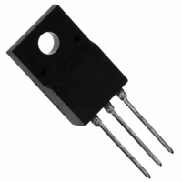
MOSFET N-CH 600V 10A TO-220SIS

2SK3569(Q,M)

Manufacturer Part Number
2SK3569(Q,M)
Description
MOSFET N-CH 600V 10A TO-220SIS
Manufacturer
Toshiba
Datasheet

Specifications of 2SK3569(Q,M)

Fet Type
MOSFET N-Channel, Metal Oxide
Fet Feature
Standard
Rds On (max) @ Id, Vgs
750 mOhm @ 5A, 10V
Drain To Source Voltage (vdss)
600V
Current - Continuous Drain (id) @ 25° C
10A
Vgs(th) (max) @ Id
4V @ 1mA
Gate Charge (qg) @ Vgs
42nC @ 10V
Input Capacitance (ciss) @ Vds
1500pF @ 25V
Power - Max
45W
Mounting Type
Through Hole
Package / Case
2-10U1B
Lead Free Status / RoHS Status
Lead free / RoHS Compliant
Other names
2SK3569(Q)
2SK3569Q
2SK3569Q
Switching Regulator Applications
Absolute Maximum Ratings
Thermal Characteristics
Low drain-source ON-resistance: R
High forward transfer admittance: |Y
Low leakage current: I
Enhancement mode: V
Drain-source voltage
Drain-gate voltage (R
Gate-source voltage
Drain current
Drain power dissipation (Tc = 25°C)
Single pulse avalanche energy
Avalanche current
Repetitive avalanche energy (Note 3)
Channel temperature
Storage temperature range
Note:
Thermal resistance, channel to case
Thermal resistance, channel to ambient
Note 1: Ensure that the channel temperature does not exceed 150℃.
Note 2: V
Note 3: Repetitive rating: pulse width limited by maximum channel temperature
This transistor is an electrostatic-sensitive device. Please handle with caution.
Using continuously under heavy loads (e.g. the application of high temperature/current/voltage and the significant change in
temperature, etc.) may cause this product to decrease in the reliability significantly even if the operating conditions (i.e.
operating temperature/current/voltage, etc.) are within the absolute maximum ratings. Please design the appropriate
reliability upon reviewing the Toshiba Semiconductor Reliability Handbook (“Handling Precautions”/“Derating Concept and
Methods”) and individual reliability data (i.e. reliability test report and estimated failure rate, etc).
Characteristics
DD
Characteristics
TOSHIBA Field Effect Transistor Silicon N Channel MOS Type (π-MOSVI)
= 90 V, T
GS
DC
Pulse (t = 1 ms)
DSS
= 20 kΩ)
th
ch
= 2.0 to 4.0 V (V
= 25°C (initial), L = 6.36 mH, I
(Note 1)
(Note 1)
(Note 2)
= 100 μA (max) (V
DS (ON)
fs
(Ta = 25°C)
| = 8.5 S (typ.)
Symbol
V
V
V
E
E
T
I
I
T
P
DGR
GSS
DSS
I
DP
AR
AS
AR
stg
D
ch
DS
R
R
D
2SK3569
Symbol
th (ch-a)
th (ch-c)
= 0.54 Ω (typ.)
= 10 V, I
DS
= 600 V)
-55 to 150
D
Rating
600
600
±30
363
150
4.5
= 1 mA)
10
40
45
10
AR
1
Max
2.78
62.5
= 10 A, R
Unit
mJ
mJ
°C
°C
°C/W
°C/W
W
G
V
V
V
A
A
Unit
= 25 Ω
Weight : 1.7 g (typ.)
JEDEC
JEITA
TOSHIBA
1
1: Gate
2: Drain
3: Source
2-10U1B
SC-67
2010-01-29
2SK3569
2
3
Unit: mm

Related parts for 2SK3569(Q,M)

2SK3569(Q,M) Summary of contents

Page 1

... Please design the appropriate reliability upon reviewing the Toshiba Semiconductor Reliability Handbook (“Handling Precautions”/“Derating Concept and Methods”) and individual reliability data (i.e. reliability test report and estimated failure rate, etc). ...

Page 2

... Labels. Not underlined: [[Pb]]/INCLUDES > MCV Underlined: [[G]]/RoHS COMPATIBLE or [[G]]/RoHS [[Pb]] Please contact your TOSHIBA sales representative for details as to environmental matters such as the RoHS compatibility of Product. The RoHS is the Directive 2002/95/EC of the European Parliament and of the Council of 27 January 2003 on the restriction of the use of certain hazardous substances in electrical and electronic equipment ...

Page 3

I – COMMON SOURCE 5 25°C PULSE TEST 8 10 DRAIN-SOURCE VOLTAGE – ...

Page 4

R – (ON) 2.5 COMMON SOURCE PULSE TEST 2 10A 1 0.5 0 −80 − CASE TEMPERATURE Tc (°C) CAPACITANCE – 10000 1000 ...

Page 5

Duty=0.5 Duty=0.5 0.2 0.1 0.1 0.05 0.02 0.01 0.01 SINGLE PULSE 0.001 10μ 100μ SAFE OPERATING AREA 100 I D max (PULSED) * 100 μ max (CONTINUOUS OPERATION Tc = ...

Page 6

... Product shall not be used for or incorporated into any products or systems whose manufacture, use, or sale is prohibited under any applicable laws or regulations. • The information contained herein is presented only as guidance for Product use. No responsibility is assumed by TOSHIBA for any infringement of patents or any other intellectual property rights of third parties that may result from the use of Product. No license to any intellectual property right is granted by this document, whether express or implied, by estoppel or otherwise. • ...

Related keywords