NDF06N60ZG ON Semiconductor, NDF06N60ZG Datasheet

MOSFET N-CH 600V 6A TO-220FP

NDF06N60ZG

Manufacturer Part Number
NDF06N60ZG
Description
MOSFET N-CH 600V 6A TO-220FP
Manufacturer
ON Semiconductor
Datasheet

Specifications of NDF06N60ZG

Fet Type
MOSFET N-Channel, Metal Oxide
Fet Feature
Standard
Rds On (max) @ Id, Vgs
1.2 Ohm @ 3A, 10V
Drain To Source Voltage (vdss)
600V
Current - Continuous Drain (id) @ 25° C
6A
Vgs(th) (max) @ Id
4.5V @ 100µA
Gate Charge (qg) @ Vgs
31nC @ 10V
Input Capacitance (ciss) @ Vds
923pF @ 25V
Power - Max
31W
Mounting Type
Through Hole
Package / Case
TO-220-3 Full Pack (Straight Leads)
Transistor Polarity
N-Channel
Resistance Drain-source Rds (on)
0.98 Ohms
Gate Charge Qg
31 nC
Forward Transconductance Gfs (max / Min)
5 S
Drain-source Breakdown Voltage
600 V
Continuous Drain Current
6 A
Power Dissipation
31 W
Maximum Operating Temperature
+ 150 C
Mounting Style
Through Hole
Minimum Operating Temperature
- 55 C
Lead Free Status / RoHS Status
Lead free / RoHS Compliant

Available stocks

Company
Part Number
Manufacturer
Quantity
Price
Part Number:
NDF06N60ZG
Manufacturer:
ON
Quantity:
1 450
Part Number:
NDF06N60ZG
Manufacturer:
ON
Quantity:
40
Part Number:
NDF06N60ZG
Manufacturer:
ON
Quantity:
1 000
Part Number:
NDF06N60ZG
Manufacturer:
ON/安森美
Quantity:
20 000
Company:
Part Number:
NDF06N60ZG
Quantity:
101
Company:
Part Number:
NDF06N60ZG
Quantity:
15 087
NDF06N60Z, NDP06N60Z
N-Channel Power MOSFET
600 V, 0.98 W
Features
Stresses exceeding Maximum Ratings may damage the device. Maximum
Ratings are stress ratings only. Functional operation above the Recommended
Operating Conditions is not implied. Extended exposure to stresses above the
Recommended Operating Conditions may affect device reliability.
1. Surface mounted on FR4 board using 1″ sq. pad size, 1 oz cu
2. Limited by maximum junction temperature
3. I
ABSOLUTE MAXIMUM RATINGS
© Semiconductor Components Industries, LLC, 2010
April, 2010 − Rev. 2
Drain−to−Source Voltage
Continuous Drain Current,
Continuous Drain Current
Pulsed Drain Current,
Power Dissipation, R
Gate−to−Source Voltage
Single Pulse Avalanche
ESD (HBM)
RMS Isolation Voltage
(t = 0.3 sec., R.H. ≤ 30%,
T
Peak Diode Recovery
Continuous Source
Maximum Temperature for
Operating Junction and
Storage Temperature Range
Compliant
Low ON Resistance
Low Gate Charge
100% Avalanche Tested
These Devices are Pb−Free, Halogen Free/BFR Free and are RoHS
A
SD
R
T
V
(Note 1)
Energy, L = 6.3 mH,
I
(JESD22−A114)
Current (Body Diode)
Soldering Leads
D
= 25°C) (Figure 13)
A
GS
qJC
= 6.0 A
= 6.0 A, di/dt ≤ 100 A/ms, V
= 100°C, R
@ 10 V
Rating
qJC
qJC
Symbol
T
V
V
dv/dt
V
J
V
E
I
DD
P
T
, T
DSS
DM
I
I
ISO
I
esd
GS
D
D
AS
S
D
L
stg
≤ BV
(T
C
NDF06N60Z
DSS
= 25°C unless otherwise noted)
, T
4500
31
J
= +150°C
6.0 (Note 2)
3.8 (Note 2)
4.5 (Note 3)
20 (Note 2)
−55 to 150
3000
600
±30
260
113
6.0
NDP06N60Z
113
1
V/ns
Unit
mJ
°C
°C
W
V
A
A
A
V
V
V
A
NDF06N60ZG
NDP06N60ZG
Device
CASE 221D
CASE 221A
TO−220AB
TO−220FP
600 V
V
STYLE 1
STYLE 5
DSS
ORDERING INFORMATION
A
Y
WW
G
http://onsemi.com
TO−220FP
TO−220AB
Package
= Location Code
= Year
= Work Week
= Pb−Free Package
G (1)
Publication Order Number:
R
Gate
DS(ON)
NDF06N60ZG
NDP06N60ZG
MARKING
DIAGRAM
N−Channel
0.98 Ω
AYWW
Drain
In Development
(TYP) @ 3 A
D (2)
50 Units/Rail
or
NDF06N60Z/D
Shipping
Source
S (3)

Related parts for NDF06N60ZG

NDF06N60ZG Summary of contents

Page 1

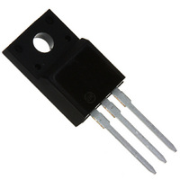
... G (1) TO−220FP CASE 221D MARKING STYLE 1 DIAGRAM NDF06N60ZG or NDP06N60ZG AYWW Gate TO−220AB CASE 221A STYLE 5 Drain A = Location Code Y = Year WW = Work Week G = Pb−Free Package ORDERING INFORMATION Device Package Shipping NDF06N60ZG TO−220FP 50 Units/Rail NDP06N60ZG TO−220AB In Development Publication Order Number: NDF06N60Z/D S (3) Source ...

Page 2

THERMAL RESISTANCE Parameter Junction−to−Case (Drain) Junction−to−Ambient Steady State (Note 4) ELECTRICAL CHARACTERISTICS Characteristic OFF CHARACTERISTICS Drain−to−Source Breakdown Voltage Breakdown Voltage Temperature Coefficient Drain−to−Source Leakage Current Gate−to−Source Forward Leakage ON CHARACTERISTICS (Note 5) Static Drain−to−Source On−Resistance Gate Threshold Voltage Forward Transconductance ...

Page 3

25° DRAIN−TO−SOURCE VOLTAGE (V) DS Figure 1. On−Region Characteristics 2 1 ...

Page 4

C iss 1000 C 500 oss C rss 100 V , DRAIN−TO−SOURCE VOLTAGE (V) DS Figure 7. Capacitance Variation 1000 V = 300 ...

Page 5

... Figure 12. Thermal Impedance for NDF06N60Z Figure 13. Mounting Position for Isolation Test Measurement made between leads and heatsink with all leads shorted together. *For additional mounting information, please download the ON Semiconductor Soldering and Mounting Techniques Reference Manual, SOLDERRM/D. TYPICAL CHARACTERISTICS 0.001 ...

Page 6

... Opportunity/Affirmative Action Employer. This literature is subject to all applicable copyright laws and is not for resale in any manner. PUBLICATION ORDERING INFORMATION LITERATURE FULFILLMENT: Literature Distribution Center for ON Semiconductor P.O. Box 5163, Denver, Colorado 80217 USA Phone: 303−675−2175 or 800−344−3860 Toll Free USA/Canada Fax: 303− ...

Related keywords