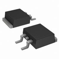
NTB30N06LT4G ON Semiconductor, NTB30N06LT4G Datasheet

MOSFET N-CH 60V 30A D2PAK

NTB30N06LT4G

Manufacturer Part Number
NTB30N06LT4G
Description
MOSFET N-CH 60V 30A D2PAK
Manufacturer
ON Semiconductor
Type
Power MOSFETr
Datasheet

Specifications of NTB30N06LT4G

Fet Type
MOSFET N-Channel, Metal Oxide
Fet Feature
Logic Level Gate
Rds On (max) @ Id, Vgs
46 mOhm @ 15A, 5V
Drain To Source Voltage (vdss)
60V
Current - Continuous Drain (id) @ 25° C
30A
Vgs(th) (max) @ Id
2V @ 250µA
Gate Charge (qg) @ Vgs
32nC @ 5V
Input Capacitance (ciss) @ Vds
1150pF @ 25V
Power - Max
88.2W
Mounting Type
Surface Mount
Package / Case
D²Pak, TO-263 (2 leads + tab)
Configuration
Single
Transistor Polarity
N-Channel
Resistance Drain-source Rds (on)
0.046 Ohm @ 5 V
Forward Transconductance Gfs (max / Min)
21 S
Drain-source Breakdown Voltage
60 V
Gate-source Breakdown Voltage
+/- 15 V
Continuous Drain Current
30 A
Power Dissipation
88200 mW
Maximum Operating Temperature
+ 175 C
Mounting Style
SMD/SMT
Minimum Operating Temperature
- 55 C
Number Of Elements
1
Polarity
N
Channel Mode
Enhancement
Drain-source On-res
0.046Ohm
Drain-source On-volt
60V
Gate-source Voltage (max)
±15V
Operating Temp Range
-55C to 175C
Operating Temperature Classification
Military
Mounting
Surface Mount
Pin Count
2 +Tab
Package Type
D2PAK
Lead Free Status / RoHS Status
Lead free / RoHS Compliant
Other names
NTB30N06LT4GOS

Available stocks

Company
Part Number
Manufacturer
Quantity
Price
Part Number:
NTB30N06LT4G
Manufacturer:
ON
Quantity:
12 500
Part Number:
NTB30N06LT4G
Manufacturer:
ON SEMICONDUCTOR
Quantity:
30 000
NTP30N06L, NTB30N06L
Power MOSFET
30 Amps, 60 Volts, Logic Level,
N−Channel TO−220 and D
power supplies, converters and power motor controls and bridge
circuits.
Features
Typical Applications
Maximum ratings are those values beyond which device damage can occur.
Maximum ratings applied to the device are individual stress limit values (not
normal operating conditions) and are not valid simultaneously. If these limits are
exceeded, device functional operation is not implied, damage may occur and
reliability may be affected.
MAXIMUM RATINGS
© Semiconductor Components Industries, LLC, 2006
January, 2006 − Rev. 4
Drain−to−Source Voltage
Drain−to−Gate Voltage (R
Gate−to−Source Voltage
Drain Current
Total Power Dissipation @ T
Derate above 25°C
Operating and Storage Temperature Range
Single Pulse Drain−to−Source Avalanche
Energy − Starting T
(V
I
Thermal Resistance, Junction−to−Case
Maximum Lead Temperature for Soldering
Purposes, 1/8 in from case for 10 seconds
L(pk)
Designed for low voltage, high speed switching applications in
Pb−Free Packages are Available
Power Supplies
Converters
Power Motor Controls
Bridge Circuits
DD
= 50 Vdc, V
= 26 A, V
− Continuous @ T
− Continuous @ T
− Single Pulse (t
DS
− Continuous
− Non−Repetitive (t
GS
= 60 Vdc)
Rating
J
= 5.0 Vdc, L = 0.3 mH
= 25°C
(T
J
GS
p
= 25°C unless otherwise noted)
v10 ms)
A
A
A
= 10 MW)
= 25°C
= 100°C
= 25°C
p
v10 ms)
2
PAK
Symbol
T
V
V
R
J
V
V
E
I
P
DGR
, T
T
DSS
DM
I
I
qJC
GS
GS
D
D
AS
D
L
stg
−55 to
Value
+175
"15
"20
88.2
0.59
101
260
1.7
60
60
30
15
90
1
W/°C
°C/W
Unit
Vdc
Vdc
Vdc
Adc
Apk
mJ
°C
°C
W
See detailed ordering and shipping information in the package
dimensions section on page 5 of this data sheet.
1
1
2
3
3
2
30 AMPERES, 60 VOLTS
NTx30N06L = Device Code
x
A
Y
WW
G
ORDERING INFORMATION
4
G
R
http://onsemi.com
DS(on)
4
CASE 221A
CASE 418B
STYLE 5
TO−220
STYLE 2
D
= P or B
= Assembly Location
= Year
= Work Week
= Pb−Free Package
2
D
PAK
Publication Order Number:
= 46 mW
S
N−Channel
Gate
Gate
DIAGRAMS
1
MARKING
NTx30N06LG
AYWW
1
NTx
30N06LG
AYWW
NTP30N06L/D
Drain
Drain
Drain
Drain
4
4
2
2
3
Source
3
Source

Related parts for NTB30N06LT4G

NTB30N06LT4G Summary of contents

Page 1

NTP30N06L, NTB30N06L Power MOSFET 30 Amps, 60 Volts, Logic Level, N−Channel TO−220 and D Designed for low voltage, high speed switching applications in power supplies, converters and power motor controls and bridge circuits. Features • Pb−Free Packages are Available Typical ...

Page 2

ELECTRICAL CHARACTERISTICS Characteristic OFF CHARACTERISTICS Drain−to−Source Breakdown Voltage (Note 1) = 250 mAdc Vdc Temperature Coefficient (Positive) Zero Gate Voltage Drain Current ( Vdc Vdc ...

Page 3

5 DRAIN−TO−SOURCE VOLTAGE (VOLTS) DS Figure 1. On−Region Characteristics 0 0.08 ...

Page 4

2400 2000 C iss 1600 1200 C rss 800 400 GATE−TO−SOURCE OR DRAIN−TO−SOURCE VOLTAGE (VOLTS) Figure 7. Capacitance Variation ...

Page 5

... Figure 14. Diode Reverse Recovery Waveform ORDERING INFORMATION Device NTP30N06L NTP30N06LG NTB30N06L NTB30N06LG NTB30N06LT4 NTB30N06LT4G †For information on tape and reel specifications, including part orientation and tape sizes, please refer to our Tape and Reel Packaging Specifications Brochure, BRD8011/D. NTP30N06L, NTB30N06L P (pk DUTY CYCLE ...

Page 6

NTP30N06L, NTB30N06L PACKAGE DIMENSIONS TO−220 CASE 221A−09 ISSUE AA NOTES: SEATING 1. DIMENSIONING AND TOLERANCING PER ANSI −T− PLANE Y14.5M, ...

Page 7

... −T− SEATING PLANE 0.13 (0.005 10.66 0.42 *For additional information on our Pb−Free strategy and soldering details, please download the ON Semiconductor Soldering and Mounting Techniques Reference Manual, SOLDERRM/D. NTP30N06L, NTB30N06L PACKAGE DIMENSIONS 2 D PAK CASE 418B−04 ISSUE SOLDERING FOOTPRINT* 8 ...

Page 8

... Fax: 480−829−7709 or 800−344−3867 Toll Free USA/Canada Email: orderlit@onsemi.com NTP30N06L, NTB30N06L N. American Technical Support: 800−282−9855 Toll Free USA/Canada Japan: ON Semiconductor, Japan Customer Focus Center 2−9−1 Kamimeguro, Meguro−ku, Tokyo, Japan 153−0051 Phone: 81−3−5773−3850 http://onsemi.com 8 ON Semiconductor Website: http://onsemi ...

Related keywords