MTB2P50ET4G ON Semiconductor, MTB2P50ET4G Datasheet - Page 2
MTB2P50ET4G
Manufacturer Part Number
MTB2P50ET4G
Description
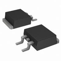
MOSFET P-CH 500V 2A D2PAK
Manufacturer
ON Semiconductor
Datasheet
1.MTB2P50ET4G.pdf
(8 pages)
Specifications of MTB2P50ET4G
Fet Type
MOSFET P-Channel, Metal Oxide
Fet Feature
Standard
Rds On (max) @ Id, Vgs
6 Ohm @ 1A, 10V
Drain To Source Voltage (vdss)
500V
Current - Continuous Drain (id) @ 25° C
2A
Vgs(th) (max) @ Id
4V @ 250µA
Gate Charge (qg) @ Vgs
27nC @ 10V
Input Capacitance (ciss) @ Vds
1183pF @ 25V
Power - Max
2.5W
Mounting Type
Surface Mount
Package / Case
D²Pak, TO-263 (2 leads + tab)
Lead Free Status / RoHS Status
Lead free / RoHS Compliant
Available stocks
Company
Part Number
Manufacturer
Quantity
Price
Company:

Part Number:
MTB2P50ET4G
Manufacturer:
ROHM
Quantity:
30 000
Company:
Part Number:
MTB2P50ET4G
Manufacturer:
ON
Quantity:
12 500


2. Pulse Test: Pulse Width ≤ 300 ms, Duty Cycle ≤ 2%.
3. Switching characteristics are independent of operating junction temperature.
ELECTRICAL CHARACTERISTICS
OFF CHARACTERISTICS
ON CHARACTERISTICS (Note 2)
DYNAMIC CHARACTERISTICS
SWITCHING CHARACTERISTICS (Note 3)
SOURCE−DRAIN DIODE CHARACTERISTICS
INTERNAL PACKAGE INDUCTANCE
Drain−Source Breakdown Voltage
Zero Gate Voltage Drain Current
Gate−Body Leakage Current (V
Gate Threshold Voltage
Static Drain−Source On−Resistance (V
Drain−Source On−Voltage (V
Forward Transconductance (V
Input Capacitance
Output Capacitance
Reverse Transfer Capacitance
Turn−On Delay Time
Rise Time
Turn−Off Delay Time
Fall Time
Gate Charge (See Figure 8)
Forward On−Voltage (Note 2)
Reverse Recovery Time
(See Figure 14)
Reverse Recovery Stored Charge
Internal Drain Inductance
Internal Source Inductance
(V
Temperature Coefficient (Positive)
(V
(V
(V
Temperature Coefficient (Negative)
(I
(I
(Measured from the drain lead 0.25″ from package to center of die)
(Measured from the source lead 0.25″ from package to source bond pad)
D
D
GS
DS
DS
DS
= 2.0 Adc)
= 1.0 Adc, T
= 0 Vdc, I
= 500 Vdc, V
= 500 Vdc, V
= V
GS
, I
D
D
= 250 mAdc)
J
= 250 mAdc)
= 125°C)
GS
GS
= 0 Vdc)
= 0 Vdc, T
GS
DS
GS
= 10 Vdc)
Characteristic
= 15 Vdc, I
= ± 20 Vdc, V
J
(V
= 125°C)
(V
DS
(I
GS
DS
S
(T
= 400 Vdc, I
= 2.0 Adc, V
= 10 Vdc, I
= 25 Vdc, V
J
(V
D
(I
(I
= 25°C unless otherwise noted)
V
DD
S
S
= 1.0 Adc)
GS
= 2.0 Adc, V
= 2.0 Adc, V
DS
= 250 Vdc, I
dI
= 10 Vdc, R
= 0)
S
/dt = 100 A/ms)
D
D
GS
GS
= 1.0 Adc)
= 2.0 Adc, V
http://onsemi.com
= 0 Vdc, T
= 0 Vdc, f = 1.0 MHz)
MTB2P50E
GS
GS
D
G
= 2.0 Adc,
= 9.1 W)
= 0 Vdc)
= 0 Vdc,
2
J
GS
= 125°C)
= 10 Vdc)
V
Symbol
R
V
V
(BR)DSS
t
t
I
I
DS(on)
C
Q
DS(on)
C
V
GS(th)
C
g
d(on)
d(off)
DSS
GSS
Q
Q
Q
Q
L
L
t
t
t
FS
oss
t
t
SD
iss
rss
RR
rr
a
b
r
D
S
f
T
1
2
3
Min
500
2.0
1.5
−
−
−
−
−
−
−
−
−
−
−
−
−
−
−
−
−
−
−
−
−
−
−
−
−
−
−
1.85
1.92
Typ
564
845
100
223
161
3.0
4.0
4.5
9.5
2.9
3.7
7.9
9.9
2.3
4.5
7.5
26
12
14
21
19
19
62
−
−
−
−
−
1183
Max
14.4
12.6
100
100
140
4.0
6.0
3.5
10
52
24
28
42
38
27
−
−
−
−
−
−
−
−
−
−
−
−
−
−
mV/°C
mV/°C
mhos
mAdc
nAdc
Unit
Vdc
Vdc
Vdc
Vdc
nC
mC
nH
nH
pF
ns
ns
W
Related parts for MTB2P50ET4G
Image
Part Number
Description
Manufacturer
Datasheet
Request
R

Part Number:
Description:
.156 HEADER & HOUSING .156 [3.96] CENTERLINE
Manufacturer:
ADAM-TECH [Adam Technologies, Inc.]
Datasheet:

Part Number:
Description:
ON Semiconductor [VOLTAGE REGULATOR]
Manufacturer:
ON Semiconductor
Datasheet:
Part Number:
Description:
357-036-542-201 CARDEDGE 36POS DL .156 BLK LOPRO
Manufacturer:
ON Semiconductor
Datasheet:
Part Number:
Description:
357-036-542-201 CARDEDGE 36POS DL .156 BLK LOPRO
Manufacturer:
ON Semiconductor
Datasheet:
Part Number:
Description:
357-036-542-201 CARDEDGE 36POS DL .156 BLK LOPRO
Manufacturer:
ON Semiconductor
Datasheet:
Part Number:
Description:
357-036-542-201 CARDEDGE 36POS DL .156 BLK LOPRO
Manufacturer:
ON Semiconductor
Datasheet:
Part Number:
Description:
357-036-542-201 CARDEDGE 36POS DL .156 BLK LOPRO
Manufacturer:
ON Semiconductor
Datasheet:
Part Number:
Description:
357-036-542-201 CARDEDGE 36POS DL .156 BLK LOPRO
Manufacturer:
ON Semiconductor
Datasheet:
Part Number:
Description:
357-036-542-201 CARDEDGE 36POS DL .156 BLK LOPRO
Manufacturer:
ON Semiconductor
Datasheet:
Part Number:
Description:
357-036-542-201 CARDEDGE 36POS DL .156 BLK LOPRO
Manufacturer:
ON Semiconductor
Datasheet:
Part Number:
Description:
357-036-542-201 CARDEDGE 36POS DL .156 BLK LOPRO
Manufacturer:
ON Semiconductor
Datasheet:
Part Number:
Description:
357-036-542-201 CARDEDGE 36POS DL .156 BLK LOPRO
Manufacturer:
ON Semiconductor
Datasheet:
Part Number:
Description:
Manufacturer:
ON Semiconductor
Datasheet:
Part Number:
Description:
Manufacturer:
ON Semiconductor
Datasheet: