MTB2P50ET4G ON Semiconductor, MTB2P50ET4G Datasheet - Page 3
MTB2P50ET4G
Manufacturer Part Number
MTB2P50ET4G
Description
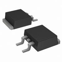
MOSFET P-CH 500V 2A D2PAK
Manufacturer
ON Semiconductor
Datasheet
1.MTB2P50ET4G.pdf
(8 pages)
Specifications of MTB2P50ET4G
Fet Type
MOSFET P-Channel, Metal Oxide
Fet Feature
Standard
Rds On (max) @ Id, Vgs
6 Ohm @ 1A, 10V
Drain To Source Voltage (vdss)
500V
Current - Continuous Drain (id) @ 25° C
2A
Vgs(th) (max) @ Id
4V @ 250µA
Gate Charge (qg) @ Vgs
27nC @ 10V
Input Capacitance (ciss) @ Vds
1183pF @ 25V
Power - Max
2.5W
Mounting Type
Surface Mount
Package / Case
D²Pak, TO-263 (2 leads + tab)
Lead Free Status / RoHS Status
Lead free / RoHS Compliant
Available stocks
Company
Part Number
Manufacturer
Quantity
Price
Company:

Part Number:
MTB2P50ET4G
Manufacturer:
ROHM
Quantity:
30 000
Company:
Part Number:
MTB2P50ET4G
Manufacturer:
ON
Quantity:
12 500


3.5
2.5
1.5
0.5
1.5
0.5
10
4
3
2
1
0
8
6
4
2
0
2
1
− 50
0
0
Figure 3. On−Resistance versus Drain Current
V
T
GS
Figure 5. On−Resistance Variation with
J
− 25
0.5
V
I
= 25°C
D
Figure 1. On−Region Characteristics
GS
4
= 10 V
= 1 A
V
= 10 V
DS
, DRAIN−TO−SOURCE VOLTAGE (VOLTS)
1
T
0
J
, JUNCTION TEMPERATURE (°C)
8
I
D
, DRAIN CURRENT (AMPS)
and Temperature
1.5
25
Temperature
12
T
J
= 100°C
50
2
25°C
− 55°C
V
TYPICAL ELECTRICAL CHARACTERISTICS
16
GS
2.5
= 10 V
75
20
100
3
4 V
6 V
5 V
24
125
3.5
http://onsemi.com
8 V
7 V
MTB2P50E
150
28
4
3
1000
5.75
5.25
4.75
4.25
100
3.5
2.5
1.5
0.5
5.5
4.5
10
4
3
2
1
0
6
5
4
1
0
2
0
Figure 4. On−Resistance versus Drain Current
V
2.5
50
DS
V
0.5
T
GS
J
Figure 6. Drain−To−Source Leakage
≥ 10 V
Figure 2. Transfer Characteristics
= 25°C
= 0 V
V
V
100
DS
GS
3
, DRAIN−TO−SOURCE VOLTAGE (VOLTS)
, GATE−TO−SOURCE VOLTAGE (VOLTS)
1
Current versus Voltage
150 200
3.5
I
D
, DRAIN CURRENT (AMPS)
and Gate Voltage
V
1.5
GS
4
= 10 V
T
100°C
25°C
250
4.5
J
2
= 125°C
15 V
T
J
300
= − 55°C
5
2.5
350
5.5
3
400
6
3.5
100°C
25°C
450
6.5
500
7
4
Related parts for MTB2P50ET4G
Image
Part Number
Description
Manufacturer
Datasheet
Request
R

Part Number:
Description:
.156 HEADER & HOUSING .156 [3.96] CENTERLINE
Manufacturer:
ADAM-TECH [Adam Technologies, Inc.]
Datasheet:

Part Number:
Description:
ON Semiconductor [VOLTAGE REGULATOR]
Manufacturer:
ON Semiconductor
Datasheet:
Part Number:
Description:
357-036-542-201 CARDEDGE 36POS DL .156 BLK LOPRO
Manufacturer:
ON Semiconductor
Datasheet:
Part Number:
Description:
357-036-542-201 CARDEDGE 36POS DL .156 BLK LOPRO
Manufacturer:
ON Semiconductor
Datasheet:
Part Number:
Description:
357-036-542-201 CARDEDGE 36POS DL .156 BLK LOPRO
Manufacturer:
ON Semiconductor
Datasheet:
Part Number:
Description:
357-036-542-201 CARDEDGE 36POS DL .156 BLK LOPRO
Manufacturer:
ON Semiconductor
Datasheet:
Part Number:
Description:
357-036-542-201 CARDEDGE 36POS DL .156 BLK LOPRO
Manufacturer:
ON Semiconductor
Datasheet:
Part Number:
Description:
357-036-542-201 CARDEDGE 36POS DL .156 BLK LOPRO
Manufacturer:
ON Semiconductor
Datasheet:
Part Number:
Description:
357-036-542-201 CARDEDGE 36POS DL .156 BLK LOPRO
Manufacturer:
ON Semiconductor
Datasheet:
Part Number:
Description:
357-036-542-201 CARDEDGE 36POS DL .156 BLK LOPRO
Manufacturer:
ON Semiconductor
Datasheet:
Part Number:
Description:
357-036-542-201 CARDEDGE 36POS DL .156 BLK LOPRO
Manufacturer:
ON Semiconductor
Datasheet:
Part Number:
Description:
357-036-542-201 CARDEDGE 36POS DL .156 BLK LOPRO
Manufacturer:
ON Semiconductor
Datasheet:
Part Number:
Description:
Manufacturer:
ON Semiconductor
Datasheet:
Part Number:
Description:
Manufacturer:
ON Semiconductor
Datasheet: