MTB2P50ET4G ON Semiconductor, MTB2P50ET4G Datasheet - Page 6
MTB2P50ET4G
Manufacturer Part Number
MTB2P50ET4G
Description
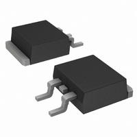
MOSFET P-CH 500V 2A D2PAK
Manufacturer
ON Semiconductor
Datasheet
1.MTB2P50ET4G.pdf
(8 pages)
Specifications of MTB2P50ET4G
Fet Type
MOSFET P-Channel, Metal Oxide
Fet Feature
Standard
Rds On (max) @ Id, Vgs
6 Ohm @ 1A, 10V
Drain To Source Voltage (vdss)
500V
Current - Continuous Drain (id) @ 25° C
2A
Vgs(th) (max) @ Id
4V @ 250µA
Gate Charge (qg) @ Vgs
27nC @ 10V
Input Capacitance (ciss) @ Vds
1183pF @ 25V
Power - Max
2.5W
Mounting Type
Surface Mount
Package / Case
D²Pak, TO-263 (2 leads + tab)
Lead Free Status / RoHS Status
Lead free / RoHS Compliant
Available stocks
Company
Part Number
Manufacturer
Quantity
Price
Company:

Part Number:
MTB2P50ET4G
Manufacturer:
ROHM
Quantity:
30 000
Company:
Part Number:
MTB2P50ET4G
Manufacturer:
ON
Quantity:
12 500


0.01
0.1
10
1
0.1
Figure 14. Diode Reverse Recovery Waveform
0.01
0.1
V
SINGLE PULSE
T
Figure 11. Maximum Rated Forward Biased
1.0E−05
1
C
GS
I
S
= 25°C
= 20 V
0.1
0.2
D = 0.5
V
DS
, DRAIN−TO−SOURCE VOLTAGE (VOLTS)
t
p
SINGLE PULSE
1
Safe Operating Area
0.01
di/dt
0.02
1.0E−04
t
a
0.05
R
THERMAL LIMIT
PACKAGE LIMIT
10
DS(on)
t
rr
t
100 ms
b
I
S
LIMIT
0.25 I
1 ms
10 ms
S
100
1.0E−03
SAFE OPERATING AREA
10 ms
Figure 13. Thermal Response
dc
http://onsemi.com
TIME
MTB2P50E
1000
6
t, TIME (s)
1.0E−02
2.5
2.0
1.5
0.5
P
80
60
40
20
(pk)
3
1
0
25
0
DUTY CYCLE, D = t
25
Figure 12. Maximum Avalanche Energy versus
t
1
Figure 15. D
t
2
T
50
R
Board material = 0.065 mil FR−4
Mounted on the minimum recommended footprint
Collector/Drain Pad Size ≈ 450 mils x 350 mils
J
, STARTING JUNCTION TEMPERATURE (°C)
Starting Junction Temperature
qJA
50
1.0E−01
T
= 50°C/W
A
, AMBIENT TEMPERATURE (°C)
1
/t
2
2
PAK Power Derating Curve
75
75
R
D CURVES APPLY FOR POWER
PULSE TRAIN SHOWN
READ TIME AT t
T
J(pk)
qJC
(t) = r(t) R
− T
C
100
1.0E+00
= P
100
qJC
(pk)
1
R
qJC
(t)
125
125
I
D
= 2 A
1.0E+01
150
150
Related parts for MTB2P50ET4G
Image
Part Number
Description
Manufacturer
Datasheet
Request
R

Part Number:
Description:
.156 HEADER & HOUSING .156 [3.96] CENTERLINE
Manufacturer:
ADAM-TECH [Adam Technologies, Inc.]
Datasheet:

Part Number:
Description:
ON Semiconductor [VOLTAGE REGULATOR]
Manufacturer:
ON Semiconductor
Datasheet:
Part Number:
Description:
357-036-542-201 CARDEDGE 36POS DL .156 BLK LOPRO
Manufacturer:
ON Semiconductor
Datasheet:
Part Number:
Description:
357-036-542-201 CARDEDGE 36POS DL .156 BLK LOPRO
Manufacturer:
ON Semiconductor
Datasheet:
Part Number:
Description:
357-036-542-201 CARDEDGE 36POS DL .156 BLK LOPRO
Manufacturer:
ON Semiconductor
Datasheet:
Part Number:
Description:
357-036-542-201 CARDEDGE 36POS DL .156 BLK LOPRO
Manufacturer:
ON Semiconductor
Datasheet:
Part Number:
Description:
357-036-542-201 CARDEDGE 36POS DL .156 BLK LOPRO
Manufacturer:
ON Semiconductor
Datasheet:
Part Number:
Description:
357-036-542-201 CARDEDGE 36POS DL .156 BLK LOPRO
Manufacturer:
ON Semiconductor
Datasheet:
Part Number:
Description:
357-036-542-201 CARDEDGE 36POS DL .156 BLK LOPRO
Manufacturer:
ON Semiconductor
Datasheet:
Part Number:
Description:
357-036-542-201 CARDEDGE 36POS DL .156 BLK LOPRO
Manufacturer:
ON Semiconductor
Datasheet:
Part Number:
Description:
357-036-542-201 CARDEDGE 36POS DL .156 BLK LOPRO
Manufacturer:
ON Semiconductor
Datasheet:
Part Number:
Description:
357-036-542-201 CARDEDGE 36POS DL .156 BLK LOPRO
Manufacturer:
ON Semiconductor
Datasheet:
Part Number:
Description:
Manufacturer:
ON Semiconductor
Datasheet:
Part Number:
Description:
Manufacturer:
ON Semiconductor
Datasheet: