SPA11N60CFD Infineon Technologies, SPA11N60CFD Datasheet
SPA11N60CFD
Specifications of SPA11N60CFD
Available stocks


Related parts for SPA11N60CFD

SPA11N60CFD Summary of contents
Page 1
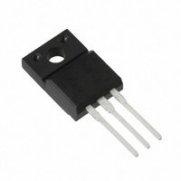
... DD 2), = 2), = /dt T =125 ° / =125 ° /dt V static >1 Hz =25 °C tot stg page 1 SPA11N60CFD Product Summary DS(on),max PG-TO220-3-31 0) Marking 11N60CFD Value =50 V 340 =50 V 0.6 11 =480 =480 V, 600 ±20 ±30 33 -55 ... 150 600 V 0. Unit V/ns V/ns A/µs ...
Page 2
... GS(th =600 DSS T =25 ° =600 =150 ° = GSS = DS(on) T =25 ° = =150 ° MHz, open drain G |V |>2 DS(on)max page 2 SPA11N60CFD Values Unit min. typ. max 3.8 K 260 °C 600 - - V - 700 - 1.1 - µA - 900 - - - 100 nA - 0.38 0. 2010-12-21 ...
Page 3
... Symbol Conditions C iss = oss f =1 MHz C rss C o(er 480 V C o(tr) t d(on) V =480 = = =6.8 d(off =480 plateau while V oss DS while V oss DS page 3 SPA11N60CFD Values Unit min. typ. max. - 1200 - pF - 390 - - 7 * rising from 0 to 80% V DSS. is rising from 0 to 80% V DSS. 2010-12-21 ...
Page 4
... Rev. 1.4 Symbol Conditions =25 ° S,pulse = =25 ° =480 /dt =100 A/µ rrm Unit Symbol Value typ. K/W C 0.0000989 th1 C 0.000939 th2 C 0.00303 th3 C 0.0245 th4 C 0.951 th5 page 4 SPA11N60CFD Values Unit min. typ. max 1.0 1 140 - ns - 0.7 - µ Unit Ws/K 2010-12-21 ...
Page 5
... parameter 0.2 0.1 0.05 -1 0.02 10 0.01 single pulse - Rev. 1.4 2 Safe operating area I =f(V D parameter 120 160 T [° Typ. output characteristics I =f(V D parameter [s] p page 5 SPA11N60CFD ); T =25 ° limited by on-state resistance [ =25 ° 10µ µs 10 µs 100 µ ...
Page 6
... DS(on 1.2 1 0.8 0 0.4 0.2 0 -60 -20 20 Rev. 1.4 6 Typ. drain-source on-state resistance R DS(on) parameter Typ. transfer characteristics = =f(V D parameter: T typ 60 100 140 180 T [°C] j page 6 SPA11N60CFD =f =150 ° 1.8 1.6 1.4 5 0.8 0.6 0 |>2 DS(on)max [V] GS ...
Page 7
... T j(start Rev. 1.4 10 Forward characteristics of reverse diode I =f(V F parameter: T 480 V 120 [nC] gate 12 Avalanche energy E =f °C 125 ° [µs] AR page 7 SPA11N60CFD ) ° 150 °C 25 ° 350 300 250 200 150 100 100 T [°C] j 150 °C, 98% 1.5 2 140 180 2010-12-21 ...
Page 8
... E = f(V ) oss 100 200 Rev. 1.4 14 Typ. capacitances C =f(V 60 100 140 180 T [° Typ. reverse recovery charge Q =f(T rr 300 400 500 600 V [V] DS page 8 SPA11N60CFD ); MHz Ciss Coss 1 Crss 100 200 300 V [V] DS );parameter 1.2 1.1 1 0.9 0.8 0.7 0 [°C] ...
Page 9
... A/µ 1.2 1 0.8 0.6 125 °C 0.4 25 °C 0 Rev. 1.4 18 Typ. reverse recovery charge Q =f(di /dt ); parameter [A] S page 9 SPA11N60CFD = 1.6 125 °C 1.5 1.4 1.3 1.2 1.1 25 °C 1 0.9 0.8 0.7 0.6 100 300 500 di/ dt [A/µs] 700 900 2010-12-21 ...
Page 10
... Definition of diode switching characteristics Rev. 1.4 page 10 SPA11N60CFD 2010-12-21 ...
Page 11
... PG-TO-220-3-31 (FullPAK) Rev. 1.4 page 11 SPA11N60CFD 2010-12-21 ...
Page 12
... Life support devices or systems are intended to be implanted in the human body support and/or maintain and sustain and/or protect human life. If they fail reasonable to assume that the health of the user or other persons may be endangered. Rev. 1.4 page 12 SPA11N60CFD 2010-12-21 ...