BSS110 Fairchild Semiconductor, BSS110 Datasheet - Page 4
BSS110
Manufacturer Part Number
BSS110
Description
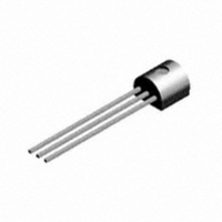
MOSFET P-CH 50V 170MA TO92
Manufacturer
Fairchild Semiconductor
Datasheet
1.BSS110.pdf
(7 pages)
Specifications of BSS110
Fet Type
MOSFET P-Channel, Metal Oxide
Fet Feature
Logic Level Gate
Rds On (max) @ Id, Vgs
10 Ohm @ 170mA, 10V
Drain To Source Voltage (vdss)
50V
Current - Continuous Drain (id) @ 25° C
170mA
Vgs(th) (max) @ Id
2V @ 1mA
Input Capacitance (ciss) @ Vds
40pF @ 25V
Power - Max
630mW
Mounting Type
Through Hole
Package / Case
TO-92-3 (Standard Body), TO-226
Lead Free Status / RoHS Status
Contains lead / RoHS non-compliant
Gate Charge (qg) @ Vgs
-
Available stocks
Company
Part Number
Manufacturer
Quantity
Price
Company:

Part Number:
BSS110
Manufacturer:
FSC
Quantity:
11 830
Company:
Part Number:
BSS110
Manufacturer:
NXPLIPS
Quantity:
5 510


Typical Electrical Characteristics
V
GS
7 0
5 0
3 0
2 0
1 0
5
3
2
1 .0 5
0 .9 5
0 .1
1 .1
0 .9
1
Figure 9. Capacitance Characteristics
Figure 11. Switching Test Circuit
-50
I
D
0 .2
R
= -250µA
Figure 7. Breakdown Voltage
-25
f = 1 MHz
V
Variation with Temperature
GEN
GS
-V
= 0V
0 .5
DS
T
0
J
, DRA IN TO SOURCE VOLTAGE (V)
, JUNCTION TEMPERATURE (°C)
V
IN
G
1
2 5
2
5 0
D
S
V
DD
7 5
5
R
L
1 0 0
DUT
1 0
(continued)
1 2 5
2 0
C iss
C oss
V
C rss
3 0
OUT
1 5 0
5 0
V
Figure 8. Body Diode Forward Voltage
t
V
OUT
0.005
0.001
d(on)
IN
0.05
0.01
0.5
0.2
0.1
1 0
1
10%
8
6
4
2
0
Figure 10. Gate Charge Characteristics
0.2
0
V
Figure 12. Switching Waveforms
GS
I
D
T = 125°C
= 0 V
J
= -0.13A
0.4
t
-V
50%
Current and Temperature
on
SD
10%
Variation with Source
, BODY DIODE FORWARD VOLTAGE (V)
0.6
0 .5
t
90%
PULSE W IDTH
r
25°C
Q
0.8
g
, GATE CHARGE (nC)
t
1
d(off)
1
V
-55°C
DS
1.2
= -10V
50%
BSS84 Rev. C2 / BSS110. Rev. A3
90%
1 .5
1.4
-20V
t
10%
off
90%
-40V
1.6
INVERTED
t
f
2
Related parts for BSS110
Image
Part Number
Description
Manufacturer
Datasheet
Request
R

Part Number:
Description:
Fairchild Semiconductor [IGBT MODULE]
Manufacturer:
Fairchild Semiconductor
Datasheet:

Part Number:
Description:
Discrete Semiconductor Modules
Manufacturer:
Fairchild Semiconductor
Part Number:
Description:
Discrete Semiconductor Modules
Manufacturer:
Fairchild Semiconductor
Part Number:
Description:
This N-Channel MOSFET is produced using Fairchild Semiconductor’s advanced Power Trench® process
Manufacturer:
Fairchild Semiconductor
Datasheet:
Part Number:
Description:
This N-Channel MOSFET is produced using Fairchild Semiconductor’s advanced Power Trench® process
Manufacturer:
Fairchild Semiconductor
Datasheet:
Part Number:
Description:
This N-Channel MOSFET is produced using Fairchild Semiconductor’s advanced PowerTrench® process
Manufacturer:
Fairchild Semiconductor
Datasheet:
Part Number:
Description:
This N-Channel MOSFET is produced using Fairchild Semiconductor’s advanced PowerTrench® process
Manufacturer:
Fairchild Semiconductor
Datasheet:
Part Number:
Description:
This N-Channel MOSFET is produced using Fairchild Semiconductor’s advanced Power Trench® process
Manufacturer:
Fairchild Semiconductor
Datasheet:
Part Number:
Description:
This N-Channel logic Level MOSFETs are produced using Fairchild Semiconductor‘s advanced Power Trench® process that has been special tailored to minimize the on-state resistance and yet maintain superior switching performance
Manufacturer:
Fairchild Semiconductor
Datasheet:
Part Number:
Description:
This N-Channel MOSFET is produced using Fairchild Semiconductor’s advanced Power Trench® process
Manufacturer:
Fairchild Semiconductor
Datasheet:
Part Number:
Description:
This N-Channel SyncFET™ is produced using Fairchild Semiconductor’s advanced PowerTrench® process
Manufacturer:
Fairchild Semiconductor
Datasheet:
Part Number:
Description:
This N-Channel SyncFET™ is produced using Fairchild Semiconductor’s advanced PowerTrench® process
Manufacturer:
Fairchild Semiconductor
Datasheet:
Part Number:
Description:
This N-Channel SyncFET™ is produced using Fairchild Semiconductor’s advanced PowerTrench® process
Manufacturer:
Fairchild Semiconductor
Datasheet:
Part Number:
Description:
This N-Channel logic Level MOSFETs are produced using Fairchild Semiconductor‘s advanced Power Trench® process that has been special tailored to minimize the on-state resistance and yet maintain superior switching performance
Manufacturer:
Fairchild Semiconductor
Datasheet:
Part Number:
Description:
This N-Channel MOSFET is produced using Fairchild Semiconductor’s advanced Power Trench® process that has been especially tailored to minimize the on-state resistance and yet maintain superior switching performance
Manufacturer:
Fairchild Semiconductor
Datasheet: