IRF840ASTRL Vishay, IRF840ASTRL Datasheet
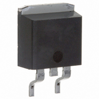
MOSFET N-CH 500V 8A D2PAK

IRF840ASTRL

Manufacturer Part Number
IRF840ASTRL
Description
MOSFET N-CH 500V 8A D2PAK
Manufacturer
Vishay
Datasheet

Specifications of IRF840ASTRL

Fet Type
MOSFET N-Channel, Metal Oxide
Fet Feature
Standard
Rds On (max) @ Id, Vgs
850 mOhm @ 4.8A, 10V
Drain To Source Voltage (vdss)
500V
Current - Continuous Drain (id) @ 25° C
8A
Vgs(th) (max) @ Id
4V @ 250µA
Gate Charge (qg) @ Vgs
38nC @ 10V
Input Capacitance (ciss) @ Vds
1018pF @ 25V
Power - Max
3.1W
Mounting Type
Surface Mount
Package / Case
D²Pak, TO-263 (2 leads + tab)
Lead Free Status / RoHS Status
Contains lead / RoHS non-compliant

Available stocks

Company
Part Number
Manufacturer
Quantity
Price
Part Number:
IRF840ASTRLPBF
Manufacturer:
VISHAY
Quantity:
300
Company:
Part Number:
IRF840ASTRLPBF
Quantity:
70 000
Note
a. See device orientation.
Notes
a. Repetitive rating; pulse width limited by maximum junction temperature (see fig. 11).
b. Starting T
c. I
d. 1.6 mm from case.
e. Uses IRF840A/SiH840A data and test conditions.
* Pb containing terminations are not RoHS compliant, exemptions may apply
Document Number: 91066
S-81412-Rev. A, 07-Jul-08
PRODUCT SUMMARY
V
R
Q
Q
Q
Configuration
ORDERING INFORMATION
Package
Lead (Pb)-free
SnPb
ABSOLUTE MAXIMUM RATINGS T
PARAMETER
Drain-Source Voltage
Gate-Source Voltage
Continuous Drain Current
Pulsed Drain Current
Linear Derating Factor
Single Pulse Avalanche Energy
Repetitive Avalanche Current
Repetitive Avalanche Energy
Maximum Power Dissipation
Peak Diode Recovery dV/dt
Operating Junction and Storage Temperature Range
Soldering Temperature
(TO-262)
DS
DS(on)
g
gs
gd
SD
I
2
(Max.) (nC)
(nC)
PAK
(nC)
(V)
≤ 8.0 A, dI/dt ≤ 100 A/µs, V
(Ω)
J
= 25 °C, L = 16 mH, R
G
a
D
(TO-263)
D
S
2
PAK
c, e
D
IRF840ASPbF
SiHF840AS-E3
IRF840AS
SiHF840AS
a
a
2
PAK (TO-263)
b
DD
V
GS
G
≤ V
= 25 Ω, I
= 10 V
DS
G
, T
N-Channel MOSFET
IRF840AS, IRF840AL, SiHF840AS, SiHF840AL
Single
J
500
≤ 150 °C.
9.0
38
18
AS
= 8.0 A (see fig. 12).
D
S
C
Power MOSFET
= 25 °C, unless otherwise noted
V
0.85
GS
D
IRF840ASTRLPbF
SiHF840ASTL-E3
IRF840ASTRL
SiHF840ASTL
at 10 V
2
PAK (TO-263)
T
T
for 10 s
C
A
= 25 °C
= 25 °C
T
T
C
C
a
a
= 100 °C
= 25 °C
FEATURES
• Low Gate Charge Q
• Improved Gate, Avalanche and Dynamic dV/dt
• Fully
• Effective C
• Lead (Pb)-free Available
APPLICATIONS
• Switch Mode Power Supply (SMPS)
• Uninterruptible Power Supply
• High Speed Power Switching
TYPICAL SMPS TOPOLOGIES
• Two Transistor Forward
• Half Bridge
• Full Bridge
a
Requirement
Ruggedness
Avalanche Voltage and Current
a
SYMBOL
Characterized
D
IRF840ASTRRPbF
SiHF840ASTR-E3
IRF840ASTRR
SiHF840ASTR
T
2
dV/dt
oss
J
PAK (TO-263)
V
V
E
E
I
I
P
, T
I
DM
AR
DS
GS
AS
AR
D
D
Specified
stg
g
a
a
Results in Simple Drive
a
a
- 55 to + 150
Capacitance
LIMIT
300
± 30
500
510
125
8.0
5.1
1.0
8.0
3.1
5.0
32
13
d
Vishay Siliconix
I
IRF840ALPbF
SiHF840AL-E3
IRF840AL
SiHF840AL
2
PAK (TO-262)
www.vishay.com
and
UNIT
W/°C
RoHS*
COMPLIANT
V/ns
mJ
mJ
°C
W
V
A
A
Available
1

Related parts for IRF840ASTRL

IRF840ASTRL Summary of contents

Page 1

... Switch Mode Power Supply (SMPS) • Uninterruptible Power Supply • High Speed Power Switching TYPICAL SMPS TOPOLOGIES • Two Transistor Forward S • Half Bridge N-Channel MOSFET • Full Bridge 2 D PAK (TO-263) a IRF840ASTRLPbF a SiHF840ASTL-E3 a IRF840ASTRL a SiHF840ASTL = 25 °C, unless otherwise noted ° 100 ° ° ° ...

Page 2

... IRF840AS, IRF840AL, SiHF840AS, SiHF840AL Vishay Siliconix THERMAL RESISTANCE RATINGS PARAMETER Maximum Junction-to-Ambient a (PCB Mount) Maximum Junction-to-Case (Drain) Note a. When mounted on 1" square PCB (FR-4 or G-10 material). SPECIFICATIONS °C, unless otherwise noted J PARAMETER Static Drain-Source Breakdown Voltage V Temperature Coefficient DS Gate-Source Threshold Voltage ...

Page 3

... T = 150 C J 0.1 0 Drain-to-Source Voltage (V) DS Fig Typical Output Characteristics Document Number: 91066 S-81412-Rev. A, 07-Jul-08 IRF840AS, IRF840AL, SiHF840AS, SiHF840AL ° 10 100 4.5V ° 10 100 Vishay Siliconix 100 ° 150 ° 50V DS 20µs PULSE WIDTH 0.1 4.0 5.0 6.0 7.0 8.0 ...

Page 4

... IRF840AS, IRF840AL, SiHF840AS, SiHF840AL Vishay Siliconix Fig Typical Capacitance vs. Drain-to-Source Voltage 7 400V 250V 100V FOR TEST CIRCUIT Total Gate Charge (nC) G Fig Typical Gate Charge vs. Gate-to-Source Voltage www.vishay.com 4 100 10 0.1 Fig Typical Source-Drain Diode Forward Voltage 100 SEE FIGURE 13 0 ...

Page 5

... RESPONSE) 0.01 0.00001 0.0001 Fig Maximum Effective Transient Thermal Impedance, Junction-to-Case Document Number: 91066 S-81412-Rev. A, 07-Jul-08 IRF840AS, IRF840AL, SiHF840AS, SiHF840AL 125 150 ° SINGLE PULSE 0.001 t , Rectangular Pulse Duration (sec) 1 Vishay Siliconix D.U. Pulse width ≤ 1 µs Duty factor ≤ 0.1 % Fig ...

Page 6

... IRF840AS, IRF840AL, SiHF840AS, SiHF840AL Vishay Siliconix D.U. 0.01 Ω Fig. 12a - Unclamped Inductive Test Circuit Fig. 12b - Unclamped Inductive Waveforms 1200 1000 800 600 400 200 100 Starting T , Junction Temperature ( C) J Fig. 12c - Maximum Avalanche Energy vs. Drain Current www.vishay.com Driver + - TOP 3 ...

Page 7

... V GS Vishay Siliconix maintains worldwide manufacturing capability. Products may be manufactured at one of several qualified locations. Reliability data for Silicon Technology and Package Reliability represent a composite of all qualified locations. For related documents such as package/tape drawings, part marking, and reliability data, see http://www.vishay.com/ppg?91066. ...

Page 8

... Vishay disclaims any and all liability arising out of the use or application of any product described herein or of any information provided herein to the maximum extent permitted by law. The product specifications do not expand or otherwise modify Vishay’ ...

Related keywords