IRFIB5N50LPBF Vishay, IRFIB5N50LPBF Datasheet
IRFIB5N50LPBF
Specifications of IRFIB5N50LPBF
Available stocks


Related parts for IRFIB5N50LPBF

IRFIB5N50LPBF Summary of contents
Page 1
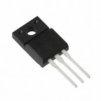
... Higher Gate Voltage Threshold Offers Improved Noise Immunity D • Lead (Pb)-free APPLICATIONS G • Zero Voltage Switching SMPS • Telecom and Server Power Supplies • Uninterruptible Power Supplies S • Motor Control Applications N-Channel MOSFET TO-220 FULLPAK IRFIB5N50LPbF SiHFIB5N50L- °C, unless otherwise noted ° 100 ° ° ...
Page 2
... IRFIB5N50L, SiHFIB5N50L Vishay Siliconix THERMAL RESISTANCE RATINGS PARAMETER Maximum Junction-to-Ambient Maximum Junction-to-Case (Drain) SPECIFICATIONS °C, unless otherwise noted J PARAMETER Static Drain-Source Breakdown Voltage V Temperature Coefficient DS Gate-Source Threshold Voltage Gate-Source Leakage Zero Gate Voltage Drain Current Drain-Source On-State Resistance Forward Transconductance Dynamic ...
Page 3
... BOTTOM 5.5V 1 0.1 20µs PULSE WIDTH Tj = 150°C 0.01 0 Drain-to-Source Voltage (V) Fig Typical Output Characteristics Document Number: 91173 S09-0063-Rev. A, 02-Feb-09 5.5V 10 100 5.5V 10 100 IRFIB5N50L, SiHFIB5N50L Vishay Siliconix 100 ° 150 ° 0 50V DS 20µs PULSE WIDTH 0.01 5.0 6.0 7.0 8 ...
Page 4
... IRFIB5N50L, SiHFIB5N50L Vishay Siliconix 100000 0V MHZ C iss = SHORTED C rss = C gd 10000 C oss = iss 1000 C oss 100 C rss Drain-to-Source Voltage (V) Fig Typical Capacitance vs. Drain-to-Source Voltage 100 200 300 V DS, Drain-to-Source Voltage (V) Fig Typical Output Capacitance Stored Energy vs. V www.vishay.com 4 100 1000 Fig Typical Gate Charge vs. Gate-to-Source Voltage ...
Page 5
... Fig Maximum Effective Transient Thermal Impedance, Junction-to-Case Document Number: 91173 S09-0063-Rev. A, 02-Feb-09 100µsec 1msec 10msec 1000 10000 125 150 0.001 0. Rectangular Pulse Duration (sec) 1 IRFIB5N50L, SiHFIB5N50L Vishay Siliconix D.U. Pulse width ≤ 1 µs Duty factor ≤ 0.1 % Fig. 11a - Switching Time Test Circuit ...
Page 6
... IRFIB5N50L, SiHFIB5N50L Vishay Siliconix 6.0 5 250µA 4.0 3.0 2.0 -75 -50 - Temperature ( °C ) Fig Threshold Voltage vs. Temperature 320 240 160 100 Starting Tj, Junction Temperature Fig Maximum Avalanche Energy vs. Drain Current D.U 0.01 Ω Fig. 15a - Unclamped Inductive Test Circuit www.vishay.com 100 ...
Page 7
... V GS Vishay Siliconix maintains worldwide manufacturing capability. Products may be manufactured at one of several qualified locations. Reliability data for Silicon Technology and Package Reliability represent a composite of all qualified locations. For related documents such as package/tape drawings, part marking, and reliability data, see www.vishay.com/ppg?91173. Document Number: 91173 S09-0063-Rev ...
Page 8
... Vishay disclaims any and all liability arising out of the use or application of any product described herein or of any information provided herein to the maximum extent permitted by law. The product specifications do not expand or otherwise modify Vishay’ ...