FDB6690S Fairchild Semiconductor, FDB6690S Datasheet
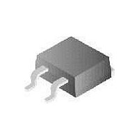
MOSFET N-CH 30V 42A TO-263AB

FDB6690S

Manufacturer Part Number
FDB6690S
Description
MOSFET N-CH 30V 42A TO-263AB
Manufacturer
Fairchild Semiconductor
Series
PowerTrench®r
Datasheet

Specifications of FDB6690S

Fet Type
MOSFET N-Channel, Metal Oxide
Fet Feature
Standard
Rds On (max) @ Id, Vgs
15.5 mOhm @ 21A, 10V
Drain To Source Voltage (vdss)
30V
Current - Continuous Drain (id) @ 25° C
42A
Vgs(th) (max) @ Id
3V @ 1mA
Gate Charge (qg) @ Vgs
15nC @ 5V
Input Capacitance (ciss) @ Vds
1238pF @ 15V
Power - Max
48W
Mounting Type
Surface Mount
Package / Case
D²Pak, TO-263 (2 leads + tab)
Configuration
Single
Transistor Polarity
N-Channel
Resistance Drain-source Rds (on)
0.00155 Ohms @ 10 V
Forward Transconductance Gfs (max / Min)
33 S
Drain-source Breakdown Voltage
30 V
Gate-source Breakdown Voltage
+/- 20 V
Continuous Drain Current
42 A
Power Dissipation
48 W
Maximum Operating Temperature
+ 150 C
Mounting Style
SMD/SMT
Minimum Operating Temperature
- 55 C
Lead Free Status / RoHS Status
Lead free / RoHS Compliant

Available stocks

Company
Part Number
Manufacturer
Quantity
Price
Part Number:
FDB6690S
Manufacturer:
FAIRCHILD
Quantity:
12 500
FDP6690S/FDB6690S
30V N-Channel PowerTrench SyncFET
General Description
This MOSFET is designed to replace a single MOSFET
and parallel Schottky diode in synchronous DC:DC
power supplies.
maximize power conversion efficiency, providing a low
R
an
monolithic SyncFET technology.
the FDP6690S/FDB6690S as the low-side switch in a
synchronous rectifier is indistinguishable from the
performance of the FDP6035AL/FDB6035AL in parallel
with a Schottky diode.
2001 Fairchild Semiconductor Corporation
DS(ON)
Absolute Maximum Ratings
Symbol
V
V
I
P
T
T
Thermal Characteristics
R
R
Package Marking and Ordering Information
D
J
L
DSS
GSS
D
, T
JC
JA
G
Device Marking
integrated
STG
D
FDB6690S
FDP6690S
and low gate charge. The FDP6690S includes
S
Drain-Source Voltage
Gate-Source Voltage
Drain Current
Total Power Dissipation @ T
Operating and Storage Junction Temperature Range
Maximum lead temperature for soldering purposes,
1/8” from case for 5 seconds
Thermal Resistance, Junction-to-Case
Thermal Resistance, Junction-to-Ambient
Schottky
This 30V MOSFET is designed to
diode
– Continuous
– Pulsed
TO-220
FDP Series
FDB6690S
FDP6690S
Device
The performance of
Parameter
using
C
= 25 C
Fairchild’s
G
T
A
Derate above 25 C
=25
S
o
C unless otherwise noted
Reel Size
Tube
13’’
(Note 1)
(Note 1)
Features
TO-263AB
FDB Series
D
21 A, 30 V.
Includes SyncFET Schottky body diode
Low gate charge (11nC typical)
High performance trench technology for extremely
High power and current handling capability
low R
DS(ON)
and fast switching
Tape width
R
R
DS(ON)
DS(ON)
–55 to +150
24mm
Ratings
n/a
62.5
140
275
0.5
2.6
30
42
48
20
= 15.5 m
= 23.0 m
G
SEPTEMBER 2001
@ V
@ V
FDP6690S/FDB6690S Rev C (W)
D
S
GS
GS
= 10 V
= 4.5 V
Quantity
800 units
45
Units
W/ C
C/W
C/W
W
V
V
A
C
C

Related parts for FDB6690S

FDB6690S Summary of contents

Page 1

... The FDP6690S includes DS(ON) an integrated Schottky diode using monolithic SyncFET technology. The performance of the FDP6690S/FDB6690S as the low-side switch in a synchronous rectifier is indistinguishable from the performance of the FDP6035AL/FDB6035AL in parallel with a Schottky diode. G TO-220 D S FDP Series Absolute Maximum Ratings ...

Page 2

... 10mA, Referenced =125 1.0 MHz GEN 21A 3.5 A (Note (Note 3 300 A/µs (Note Min Typ Max Units 140 mV/ C 500 µA 100 nA –100 –4 mV/ C 12.0 15.5 m 18.5 23.0 18.0 22 1238 pF 342 pF 104 0.51 0 FDP6690S/FDB6690S Rev C (W) ...

Page 3

... Figure 6. Body Diode Forward Voltage Variation with Source Current and Temperature. = 4.0V 4.5V 5.0V 6.0V 7.0V 8.0V 10V DRAIN CURRENT ( 125 GATE TO SOURCE VOLTAGE (V) GS Gate-to-Source Voltage -55 C 0.2 0.4 0 BODY DIODE FORWARD VOLTAGE (V) SD FDP6690S/FDB6690S Rev C ( 0.8 ...

Page 4

... Figure 10. Single Pulse Maximum 0.001 0. TIME (sec 1MHz ISS C OSS DRAIN TO SOURCE VOLTAGE (V) DS SINGLE PULSE R = 2.6°C 25°C A 0.001 0.01 0 TIME (sec) 1 Power Dissipation. R ( 2.6 ° Duty Cycle 0.1 1 FDP6690S/FDB6690S Rev C (W) ...

Page 5

... Schottky barrier diodes exhibit significant leakage at This diode high temperature and high reverse voltage. increase the power in the device. 0.01 0.001 0.0001 0.00001 0 Figure 14. SyncFET diode reverse leakage versus drain-source voltage and This will 100 REVERSE VOLTAGE (V) DS temperature. FDP6690S/FDB6690S Rev C (W) ...

Page 6

... TRADEMARKS The following are registered and unregistered trademarks Fairchild Semiconductor owns or is authorized to use and is not intended exhaustive list of all such trademarks. ACEx™ FAST Bottomless™ FASTr™ FRFET™ CoolFET™ GlobalOptoisolator™ CROSSVOLT™ GTO™ DenseTrench™ ...

Related keywords