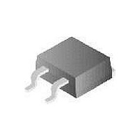
FDB6690S Fairchild Semiconductor, FDB6690S Datasheet - Page 2

FDB6690S
Manufacturer Part Number
FDB6690S
Description
MOSFET N-CH 30V 42A TO-263AB
Manufacturer
Fairchild Semiconductor
Series
PowerTrench®r
Datasheet
1.FDB6690S.pdf
(6 pages)
Specifications of FDB6690S
Fet Type
MOSFET N-Channel, Metal Oxide
Fet Feature
Standard
Rds On (max) @ Id, Vgs
15.5 mOhm @ 21A, 10V
Drain To Source Voltage (vdss)
30V
Current - Continuous Drain (id) @ 25° C
42A
Vgs(th) (max) @ Id
3V @ 1mA
Gate Charge (qg) @ Vgs
15nC @ 5V
Input Capacitance (ciss) @ Vds
1238pF @ 15V
Power - Max
48W
Mounting Type
Surface Mount
Package / Case
D²Pak, TO-263 (2 leads + tab)
Configuration
Single
Transistor Polarity
N-Channel
Resistance Drain-source Rds (on)
0.00155 Ohms @ 10 V
Forward Transconductance Gfs (max / Min)
33 S
Drain-source Breakdown Voltage
30 V
Gate-source Breakdown Voltage
+/- 20 V
Continuous Drain Current
42 A
Power Dissipation
48 W
Maximum Operating Temperature
+ 150 C
Mounting Style
SMD/SMT
Minimum Operating Temperature
- 55 C
Lead Free Status / RoHS Status
Lead free / RoHS Compliant
Available stocks
Company
Part Number
Manufacturer
Quantity
Price
Company:
Part Number:
FDB6690S
Manufacturer:
FAIRCHILD
Quantity:
12 500
Notes:
1. Pulse Test: Pulse Width < 300 s, Duty Cycle < 2.0%
2. See “SyncFET Schottky body diode characteristics” below.
Drain-Source Avalanche Ratings
W
I
Electrical Characteristics
Symbol
Off Characteristics
BV
I
I
I
On Characteristics
V
R
I
g
Dynamic Characteristics
C
C
C
Switching Characteristics
t
t
t
t
Q
Q
Q
Drain–Source Diode Characteristics
V
t
Q
AR
DSS
GSSF
GSSR
D(on)
d(on)
r
d(off)
f
rr
FS
BV
V
GS(th)
DS(on)
iss
oss
rss
SD
g
gs
gd
rr
DSS
T
GS(th)
T
DSS
J
J
DSS
Drain-Source Avalanche Energy
Drain-Source Avalanche Current
Drain–Source Breakdown Voltage
Breakdown Voltage Temperature
Coefficient
Zero Gate Voltage Drain Current
Gate–Body Leakage, Forward
Gate–Body Leakage, Reverse
Gate Threshold Voltage
Gate Threshold Voltage
Temperature Coefficient
Static Drain–Source
On–Resistance
On–State Drain Current
Forward Transconductance
Input Capacitance
Output Capacitance
Reverse Transfer Capacitance
Turn–On Delay Time
Turn–On Rise Time
Turn–Off Delay Time
Turn–Off Fall Time
Total Gate Charge
Gate–Source Charge
Gate–Drain Charge
Drain–Source Diode Forward
Voltage
Diode Reverse Recovery Time
Diode Reverse Recovery Charge
Parameter
(Note 2)
(Note 2)
(Note 2)
Single Pulse, V
T
V
I
V
V
V
V
I
V
V
V
V
V
V
f = 1.0 MHz
V
V
V
V
V
V
I
d
A
D
D
F
iF
= 25°C unless otherwise noted
GS
DS
GS
GS
DS
GS
GS
GS
GS
DS
DS
DS
GS
DS
GS
GS
GS
= 3.5 A,
= 10mA, Referenced to 25 C
= 10mA, Referenced to 25 C
/d
=10 V, I
= 0 V,
= 24 V,
= 20 V,
= –20 V, V
= V
= 10 V,
= 4.5 V, I
= 10 V,
= 10 V,
= 15 V,
= 15 V,
= 10 V,
= 15 V,
= 5 V
= 0 V,
= 0 V,
t
= 300 A/µs
Test Conditions
GS
,
D
=21 A, T
I
I
S
S
DD
I
V
V
I
I
V
I
V
D
D
D
D
D
I
R
I
= 3.5 A
= 7 A
D
D
GS
DS
DS
DS
GS
= 1mA
= 1mA
= 21 A
= 17 A
= 23 A
GEN
= 25 V, I
= 1 A,
= 21A,
= 0 V
= 0 V
= 0 V
= 10 V
= 0 V,
= 6
J
=125 C
D
(Note 1)
(Note 1)
(Note 2)
=11A
Min
30
60
1
Typ Max Units
1238
12.0
18.5
18.0
0.51
0.69
342
104
2.2
25
–4
33
11
23
13
11
21
25
9
5
4
FDP6690S/FDB6690S Rev C (W)
–100
15.5
23.0
22.5
140
100
500
0.7
11
20
18
37
23
15
3
mV/ C
mV/ C
m
µA
nA
nA
nC
nC
nC
nS
nC
mJ
pF
pF
pF
ns
ns
ns
ns
V
V
A
S
V
A


