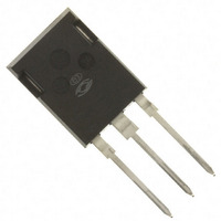
Power MOS V
mode power MOSFETs. This new technology minimizes the JFET effect,
increases packing density and reduces the on-resistance. Power MOS V
also achieves faster switching speeds through optimized gate layout.
• Identical Specifications:
• Lower Leakage
• Fast Recovery Body Diode
MAXIMUM RATINGS
STATIC ELECTRICAL CHARACTERISTICS
USA
EUROPE
Symbol
Symbol
T
R
BV
V
V
V
J
I
I
I
V
E
DS(on)
E
D(on)
GS(th)
I
,T
I
GSS
P
DSS
GSM
T
DSS
I
DM
AR
GS
AR
D
AS
DSS
D
L
STG
CAUTION: These Devices are Sensitive to Electrostatic Discharge. Proper Handling Procedures Should Be Followed.
Parameter
Drain-Source Voltage
Continuous Drain Current @ T
Pulsed Drain Current
Gate-Source Voltage Continuous
Gate-Source Voltage Transient
Total Power Dissipation @ T
Linear Derating Factor
Operating and Storage Junction Temperature Range
Lead Temperature: 0.063" from Case for 10 Sec.
Avalanche Current
Repetitive Avalanche Energy
Single Pulse Avalanche Energy
Characteristic / Test Conditions
Drain-Source Breakdown Voltage (V
On State Drain Current
Drain-Source On-State Resistance
Zero Gate Voltage Drain Current (V
Zero Gate Voltage Drain Current (V
Gate-Source Leakage Current (V
Gate Threshold Voltage (V
405 S.W. Columbia Street
Chemin de Magret
®
is a new generation of high voltage N-Channel enhancement
POWER MOS V
1
T-MAX™
1
5
2
5
(Repetitive and Non-Repetitive)
5
DS
C
APT Website - http://www.advancedpower.com
(V
1
= V
C
= 25°C
• Faster Switching
• 100% Avalanche Tested
DS
= 25°C
4
Bend, Oregon 97702 -1035
F-33700 Merignac - France
or TO-264 Package
GS
GS
> I
2
DS
DS
, I
= ±30V, V
GS
D(on)
D
(V
= V
= 0.8 V
= 0V, I
= 2.5mA)
5
GS
DSS
x R
= 10V, 0.5 I
, V
DS(on)
DSS
D
DS
= 250µA)
GS
= 0V)
®
, V
= 0V)
Max, V
GS
D[Cont.]
= 0V, T
All Ratings: T
GS
FREDFET
)
= 10V)
C
APT10M11B2VFR
Phone: (541) 382-8028
Phone: (33) 5 57 92 15 15
= 125°C)
APT10M11LVFR
100V 100A 0.011
C
®
= 25°C unless otherwise specified.
MIN
100
100
B2VFR
2
G
T-MAX™
APT10M11
-55 to 150
2500
4.16
TYP
±30
±40
100
100
400
520
300
100
50
D
S
FAX: (541) 388-0364
FAX: (33) 5 56 47 97 61
0.011
±100
1000
MAX
250
4
TO-264
LVFR
Amps
Watts
Amps
Amps
Ohms
UNIT
W/°C
UNIT
Volts
Volts
Volts
Volts
mJ
µA
nA
°C
W


