IRFP150N International Rectifier, IRFP150N Datasheet
IRFP150N
Specifications of IRFP150N
Available stocks


Related parts for IRFP150N

IRFP150N Summary of contents
Page 1
... Case-to-Sink, Flat, Greased Surface CS R Junction-to-Ambient JA www.irf.com HEXFET 10V GS @ 10V GS - 175 300 (1.6mm from case ) 10 lbf•in (1.1N•m) Typ. ––– 0.24 ––– 91503D IRFP150N ® Power MOSFET V = 100V DSS R = 0.036W DS(on 42A D TO-247AC Max. Units 140 160 W 1.1 W/° ...
Page 2
... IRFP150N Electrical Characteristics @ T Parameter V Drain-to-Source Breakdown Voltage (BR)DSS Breakdown Voltage Temp. Coefficient (BR)DSS J R Static Drain-to-Source On-Resistance DS(on) V Gate Threshold Voltage GS(th) g Forward Transconductance fs I Drain-to-Source Leakage Current DSS Gate-to-Source Forward Leakage I GSS Gate-to-Source Reverse Leakage Q Total Gate Charge g Q Gate-to-Source Charge ...
Page 3
... BOTTOM 4.5V 4.5V 10 20us PULSE WIDTH T = 175 0 Drain-to-Source Voltage (V) DS Fig 2. Typical Output Characteristics 3.0 36A 2.5 2.0 1.5 1.0 0.5 0.0 -60 -40 - 100 120 140 160 180 T , Junction Temperature ( C) J Fig 4. Normalized On-Resistance Vs. Temperature IRFP150N o 10 100 V = 10V ...
Page 4
... IRFP150N 3500 iss 3000 rss oss ds 2500 C iss 2000 1500 C oss 1000 C rss 500 Drain-to-Source Voltage (V) DS Fig 5. Typical Capacitance Vs. Drain-to-Source Voltage 1000 100 10 1 0.1 0.2 0.4 0.6 0.8 V ,Source-to-Drain Voltage (V) SD Fig 7. Typical Source-Drain Diode Forward Voltage 1MHz ...
Page 5
... Fig 11. Maximum Effective Transient Thermal Impedance, Junction-to-Case www.irf.com Fig 10a. Switching Time Test Circuit V DS 90% 125 150 175 ° 10 Fig 10b. Switching Time Waveforms 0.001 0. Rectangular Pulse Duration (sec) 1 IRFP150N D.U. 10V Pulse Width £ 1 µs Duty Factor £ 0 d(on) r ...
Page 6
... IRFP150N 20V .01 Fig 12a. Unclamped Inductive Test Circuit Fig 12b. Unclamped Inductive Waveforms Charge Fig 13a. Basic Gate Charge Waveform 6 1000 800 D R IVE R 600 + 400 200 12V Fig 13b. Gate Charge Test Circuit TOP BOTTOM 50 75 100 125 Starting T , Junction Temperature ( C) Starting Tj, Junction Temperature (° ...
Page 7
... Driver same type as D.U.T. · I controlled by Duty Factor "D" SD · D.U.T. - Device Under Test Period P.W. Waveform SD Body Diode Forward Current di/dt Waveform DS Diode Recovery dv/dt Body Diode Forward Drop Ripple for Logic Level Devices Fig 14. For N-Channel HEXFETS - + + P. Period * V =10V IRFP150N 7 ...
Page 8
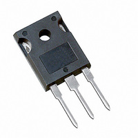
... IRFP150N Package Outline TO-247AC Outline Dimensions are shown in millimeters (inches) 15.90 (.626) 15.30 (.602 20.30 (.800) 19.70 (.775 14.80 (.583) 14.20 (.559) 2.40 (.094) 2.00 (.079) 2X 5.45 (.215) 3.40 (.133) 2X 3.00 (.118) Part Marking Information TO-247AC 3.65 (.143) 3.55 (.140) 0.25 (.010) ...
Page 9
Note: For the most current drawings please refer to the IR website at: http://www.irf.com/package/ ...