IRFZ44NL International Rectifier, IRFZ44NL Datasheet
IRFZ44NL
Specifications of IRFZ44NL
Available stocks


Related parts for IRFZ44NL

IRFZ44NL Summary of contents
Page 1
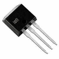
... The D for high current applications because of its low internal connection resistance and can dissipate typical surface mount application. The through-hole version (IRFZ44NL) is available for low- profile applications. Absolute Maximum Ratings Parameter 25° ...
Page 2
... IRFZ44NS/IRFZ44NL Electrical Characteristics @ T Parameter V Drain-to-Source Breakdown Voltage (BR)DSS Breakdown Voltage Temp. Coefficient (BR)DSS J R Static Drain-to-Source On-Resistance ––– DS(on) V Gate Threshold Voltage GS(th) g Forward Transconductance fs I Drain-to-Source Leakage Current DSS Gate-to-Source Forward Leakage I GSS Gate-to-Source Reverse Leakage Q Total Gate Charge ...
Page 3
... ° 0 rain-to-S ource V oltage ( Fig 1. Typical Output Characteristics ° ° µ te-to-S ource Vo ltag e ( Fig 3. Typical Transfer Characteristics www.irf.com IRFZ44NS/IRFZ44NL TOP BOTTOM 4. 0.1 Fig 2. Typical Output Characteristics 2 2.0 1.5 1.0 0 0.0 A -60 -40 - Fig 4. Normalized On-Resistance VGS 15V 10V 8.0V 7 ...
Page 4
... IRFZ44NS/IRFZ44NL iss oss rss rain-to-S ourc e V oltage ( Fig 5. Typical Capacitance Vs. Drain-to-Source Voltage ° ° 0.5 1.0 1.5 2 ource-to-D rain V oltage ( Fig 7. Typical Source-Drain Diode Forward Voltage Fig 6. Typical Gate Charge Vs ing lse 2.5 3.0 Fig 8. Maximum Safe Operating Area = FIG ...
Page 5
... D = 0.50 0.20 0.10 0.05 0.1 0.02 SINGLE PULSE 0.01 (THERMAL RESPONSE) 0.01 0.00001 0.0001 Fig 11. Maximum Effective Transient Thermal Impedance, Junction-to-Case www.irf.com IRFZ44NS/IRFZ44NL R Pulse Width Duty Factor Fig 10a. Switching Time Test Circuit V DS 90% 10% 150 175 V ° d(on) Fig 10b. Switching Time Waveforms Notes: 1 ...
Page 6
... IRFZ44NS/IRFZ44NL V DS D.U. Fig 12a. Unclamped Inductive Test Circuit Fig 12b. Unclamped Inductive Waveforms Charge Fig 13a. Basic Gate Charge Waveform 0. (BR)DSS Fig 12c. Maximum Avalanche Energy Fig 13b. Gate Charge Test Circuit TTO tarting unc tion T em perature (° Vs. Drain Current Current Regulator Same Type as D ...
Page 7
... Reverse Recovery Current D.U. Re-Applied Voltage Inductor Curent * for Logic Level Devices GS Fig 14. For N-Channel HEXFETS www.irf.com IRFZ44NS/IRFZ44NL Peak Diode Recovery dv/dt Test Circuit + Circuit Layout Considerations Low Stray Inductance Ground Plane ƒ Low Leakage Inductance Current Transformer - „ - dv/dt controlled Driver same type as D ...
Page 8
... IRFZ44NS/IRFZ44NL 2 D Pak Package Outline 1 0.54 (.4 15) 1 0.29 (.4 05) 1.4 0 (.055 ) - AX. 2 1 (.6 10) 1 (.5 80 1.40 (.0 55) 3X 1.14 (.0 45) 0 .93 (. .69 (. .08 (. .25 (. FTER IP & 4.5M , 198 TRO L LIN SIO ATSINK & Part Marking Information 2 D Pak TIO 4.69 (.1 85) 4.20 (.1 65) 1 ...
Page 9
... Package Outline TO-262 Outline Part Marking Information TO-262 www.irf.com IRFZ44NS/IRFZ44NL 9 ...
Page 10
... IRFZ44NS/IRFZ44NL Tape & Reel Information 2 D Pak IRE CTIO (. (. IRE C TIO N 33 0.00 (1 4 LLIN ILL WORLD HEADQUARTERS: 233 Kansas St., El Segundo, California 90245, USA Tel: (310) 252-7105 (. (. . . . . .10 (. .90 (. 13.50 (.532 ) 12.80 (.504 ) Data and specifications subject to change without notice. ...
Page 11
Note: For the most current drawings please refer to the IR website at: http://www.irf.com/package/ ...