IRLML2502TR International Rectifier, IRLML2502TR Datasheet
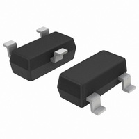
MOSFET N-CH 20V 4.2A SOT-23

IRLML2502TR

Manufacturer Part Number
IRLML2502TR
Description
MOSFET N-CH 20V 4.2A SOT-23
Manufacturer
International Rectifier
Series
HEXFET®r
Datasheet

Specifications of IRLML2502TR

Fet Type
MOSFET N-Channel, Metal Oxide
Fet Feature
Logic Level Gate
Rds On (max) @ Id, Vgs
45 mOhm @ 4.2A, 4.5V
Drain To Source Voltage (vdss)
20V
Current - Continuous Drain (id) @ 25° C
4.2A
Vgs(th) (max) @ Id
1.2V @ 250µA
Gate Charge (qg) @ Vgs
12nC @ 5V
Input Capacitance (ciss) @ Vds
740pF @ 15V
Power - Max
1.25W
Mounting Type
Surface Mount
Package / Case
SOT-23-3, TO-236-3, Micro3™, SSD3, SST3
Lead Free Status / RoHS Status
Contains lead / RoHS non-compliant
Other names
*IRLML2502TR
IRLML2502
IRLML2502
IRLML2502CT

Available stocks

Company
Part Number
Manufacturer
Quantity
Price
Part Number:
IRLML2502TR
Manufacturer:
IR
Quantity:
30 000
Part Number:
IRLML2502TR
Manufacturer:
IR
Quantity:
20 000
Part Number:
IRLML2502TR/PBF
Manufacturer:
IR
Quantity:
14 521
Part Number:
IRLML2502TRPBF
Manufacturer:
TI
Quantity:
5 195
Part Number:
IRLML2502TRPBF
Manufacturer:
International Rectifier
Quantity:
151 224
Part Number:
IRLML2502TRPBF
Manufacturer:
IR
Quantity:
20 000
Part Number:
IRLML2502TRPBF
Quantity:
3 000
Part Number:
IRLML2502TRPBF
0
Company:
Part Number:
IRLML2502TRPBF
Quantity:
60 000
Part Number:
IRLML2502TRPBF/G3E
Manufacturer:
RENESAS/瑞萨
Quantity:
20 000
Thermal Resistance
l
l
l
l
l
l
These N-Channel MOSFETs from International Rectifier
utilize advanced processing techniques to achieve extremely
low on-resistance per silicon area. This benefit, combined
with the fast switching speed and ruggedized device design
that HEXFET
the designer with an extremely efficient and reliable device
for use in battery and load management.
A thermally enhanced large pad leadframe has been
incorporated into the standard SOT-23 package to produce
a HEXFET Power MOSFET with the industry's smallest
footprint. This package, dubbed the Micro3, is ideal for
applications where printed circuit board space is at a
premium. The low profile (<1.1mm) of the Micro3 allows it
to fit easily into extremely thin application environments
such as portable electronics and PCMCIA cards. The thermal
resistance and power dissipation are the best available.
V
I
I
I
P
P
V
T
R
D
D
DM
www.irf.com
J,
DS
D
D
GS
θJA
@ T
@ T
@T
@T
T
Ultra Low On-Resistance
N-Channel MOSFET
SOT-23 Footprint
Low Profile (<1.1mm)
Available in Tape and Reel
Fast Switching
STG
A
A
A
A
= 70°C
= 25°C
= 25°C
= 70°C
power MOSFETs are well known for, provides
Drain- Source Voltage
Continuous Drain Current, V
Pulsed Drain Current 
Power Dissipation
Power Dissipation
Linear Derating Factor
Gate-to-Source Voltage
Junction and Storage Temperature Range
Maximum Junction-to-Ambientƒ
Parameter
Parameter
GS
GS
@ 4.5V
@ 4.5V
G
S
1
2
Typ.
75
HEXFET Power MOSFET
-55 to + 150
3
Micro3
Max.
D
1.25
0.01
± 12
4.2
3.4
0.8
20
33
R
DS(on)
Max.
100
V
DSS
= 0.045Ω
= 20V
Units
Units
W/°C
°C
V
A
V
1
04/30/03

Related parts for IRLML2502TR

IRLML2502TR Summary of contents

Page 1

... Low Profile (<1.1mm) Available in Tape and Reel l l Fast Switching These N-Channel MOSFETs from International Rectifier utilize advanced processing techniques to achieve extremely low on-resistance per silicon area. This benefit, combined with the fast switching speed and ruggedized device design  that HEXFET ...

Page 2

Electrical Characteristics @ T Parameter V Drain-to-Source Breakdown Voltage (BR)DSS ∆V Breakdown Voltage Temp. Coefficient /∆T (BR)DSS J R Static Drain-to-Source On-Resistance DS(on) V Gate Threshold Voltage GS(th) g Forward Transconductance fs I Drain-to-Source Leakage Current DSS Gate-to-Source Forward Leakage ...

Page 3

VGS TOP 7.00V 5.00V 4.50V 3.50V 3.00V 2.70V 2.50V BOTTOM 2.25V 2.25V 10 20µs PULSE WIDTH 0 Drain-to-Source Voltage (V) DS Fig 1. Typical Output Characteristics 100 ° ...

Page 4

1MHz iss rss gd 1000 oss ds gd 800 C iss 600 400 200 C oss ...

Page 5

Fig 9. Maximum Drain Current Vs. 1000 100 D = 0.50 0.20 0.10 10 0.05 0.02 0.01 1 SINGLE PULSE (THERMAL RESPONSE) 0.1 0.00001 0.0001 Fig 10. Maximum Effective Transient Thermal Impedance, Junction-to-Ambient www.irf.com ...

Page 6

Id = 4.0A 0.03 0.02 2.0 2.5 3.0 3.5 4.0 4.5 5.0 V GS, Gate -to -Source Voltage ( V ) Fig 11. On-Resistance Vs. Gate Voltage 6 0.30 0.20 0.10 0.00 5.5 6.0 6.5 7.0 0 Fig ...

Page 7

0.10 (.004 NOTES: 1. DIMENSIONING & TOLERANCING PER ANSI Y14.5M-1982. 2. ...

Page 8

Notes : T his part marking information applies to devices produced before 02/26/2001 EXAMPLE: T HIS IS AN IRLML6302 PART NUMBER PART NUMBER CODE REFERENCE IRLML2402 1B = IRLML2803 1C = IRLML6302 1D = IRLML5103 1E = ...

Page 9

TR FEED DIRECTION 178.00 ( 7.008 ) MAX. NOTES: 1. CONTROLLING DIMENSION : MILLIMETER. 2. OUTLINE CONFORMS TO EIA-481 & EIA-541. IR WORLD ...

Related keywords