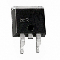
IRL1104S International Rectifier, IRL1104S Datasheet

IRL1104S
Specifications of IRL1104S
Available stocks
Related parts for IRL1104S
IRL1104S Summary of contents
Page 1
... Logic-Level Gate Drive Advanced Process Technology Surface Mount (IRL1104S) Low-profile through-hole (IRL1104L) 175°C Operating Temperature Fast Switching Fully Avalanche Rated Description Fifth Generation HEXFETs from International Rectifier utilize advanced processing techniques to achieve extremely low on-resistance per silicon area. This benefit, combined with ...
Page 2
... IRL1104S/L Electrical Characteristics @ T Parameter V Drain-to-Source Breakdown Voltage (BR)DSS Breakdown Voltage Temp. Coefficient (BR)DSS J R Static Drain-to-Source On-Resistance DS(on) V Gate Threshold Voltage GS(th) g Forward Transconductance fs I Drain-to-Source Leakage Current DSS Gate-to-Source Forward Leakage I GSS Gate-to-Source Reverse Leakage Q Total Gate Charge g Q Gate-to-Source Charge ...
Page 3
... Fig 2. Typical Output Characteristics 2 2.0 ° 175 C J 1.5 1.0 0 50V 0.0 -60 -40 -20 0 8.0 10.0 Fig 4. Normalized On-Resistance IRL1104S/L VGS 15V 10V 7.0V 5.5V 4.5V 4.0V 3.5V 2.7V 2.7V 20µs PULSE WIDTH ° 175 Drain-to-Source Voltage (V) DS 104A ...
Page 4
... IRL1104S/L 6000 1MHz iss rss gd 5000 oss ds gd 4000 C iss 3000 2000 C oss 1000 C rss Drain-to-Source Voltage (V) DS Fig 5. Typical Capacitance Vs. Drain-to-Source Voltage 1000 ° 175 C J 100 ° 0.1 0.2 0.8 1.4 V ,Source-to-Drain Voltage (V) SD Fig 7. Typical Source-Drain Diode ...
Page 5
... Fig 11. Maximum Effective Transient Thermal Impedance, Junction-to-Case www.irf.com R G Pulse Width Duty Factor Fig 10a. Switching Time Test Circuit V DS 90% 150 175 ° 10 d(on) Fig 10b. Switching Time Waveforms Notes: 1. Duty factor Peak 0.001 0. Rectangular Pulse Duration (sec) 1 IRL1104S D.U. 4.5V µ d(off ...
Page 6
... IRL1104S 0 Fig 12a. Unclamped Inductive Test Circuit Fig 12b. Unclamped Inductive Waveforms Charge Fig 13a. Basic Gate Charge Waveform 6 800 1 5V 600 400 200 Starting T , Junction Temperature ( C) Fig 12c. Maximum Avalanche Energy Same Type as D.U.T. 12V V GS Fig 13b. Gate Charge Test Circuit ...
Page 7
... Ground Plane Low Leakage Inductance Current Transformer - - dv/dt controlled Driver same type as D.U.T. I controlled by Duty Factor "D" SD D.U.T. - Device Under Test P.W. Period D = Period Waveform Body Diode Forward Current di/dt Waveform Diode Recovery dv/dt Body Diode Forward Drop Ripple 5% IRL1104S =10V * ...
Page 8
... IRL1104S Pak Package Details 1 0.54 (.4 15) 1 0.29 (.4 05) 1.4 0 (.055 ) - AX. 2 1 (.6 10) 1 (.5 80 1.40 (.0 55) 3X 1.14 (.0 45) 0 .93 (. .69 (. .08 (. .25 (. FTER IP & 4.5M , 198 TRO L LIN SIO ATSINK & Part Marking TIO 4.69 (.1 85) 4.20 (.1 65) 1.3 2 (.05 2) 1 ...
Page 9
... TO-262 Package Details Part Marking www.irf.com IRL1104S/L 9 ...
Page 10
... IRL1104S Pak Tape and Reel IRE CTIO (. (. IRE C TIO N 33 0.00 (1 4 LLIN ILL WORLD HEADQUARTERS: 233 Kansas St., El Segundo, California 90245, Tel: (310) 322 3331 IR GREAT BRITAIN: Hurst Green, Oxted, Surrey RH8 9BB, UK Tel 1883 732020 IR GERMANY: Saalburgstrasse 157, 61350 Bad Homburg Tel 6172 96590 IR FAR EAST: K& ...
Page 11
Note: For the most current drawings please refer to the IR website at: http://www.irf.com/package/ ...


