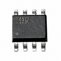
IRF7807VD1 International Rectifier, IRF7807VD1 Datasheet

IRF7807VD1
Specifications of IRF7807VD1
Available stocks
Related parts for IRF7807VD1
IRF7807VD1 Summary of contents
Page 1
... J STG Symbol R θJA R θJL PD-94078A IRF7807VD1 1 8 K/D A A/S K A/S K K/D D Top View IRF7807VD1 17mΩ 9.5nC 3.4nC 12nC Max Units 30 V ±20 8.3 A 6.6 66 2.5 W 1.6 3.5 2.2 -55 to 150 °C Typ Max Units ––– 50 °C/W ––– ...
Page 2
... IRF7807VD1 Electrical Characteristics Parameter Drain-Source Breakdown Voltage Static Drain-Source On-Resistance Gate Threshold Voltage Drain-Source Leakage Current Gate-Source Leakage Current Total Gate Charge* Pre-Vth Gate-Source Charge Post-Vth Gate-Source Charge Gate-to-Drain Charge Switch Charge ( gs2 gd Output Charge* Gate Resistance Turn-On Delay Time Rise Time ...
Page 3
... P P loss conduction ( = I P loss rms ( + Q gs2 , can be seen from *dissipated primarily in Q1 critical fac- gs2 is formed by the when multiplied by IRF7807VD1 4 Drain Current 1 Gate Voltage Drain Voltage + drive output ) 2 × R ds(on) ) × V × ( × V × × V × f oss ...
Page 4
... IRF7807VD1 For the synchronous MOSFET Q2, R portant characteristic; however, once again the im- portance of gate charge must not be overlooked since it impacts three critical areas. Under light load the MOSFET must still be turned on and off by the con- trol IC so the gate drive losses become much more significant ...
Page 5
... Fig 7. On-Resistance Vs. Gate Voltage 70 TOP 60 50 BOTTOM 0. 0. 0.8 1 Fig 8. Typical Reverse Output Characteristics IRF7807VD1 7.0A 4.0 6.0 8.0 10.0 12.0 14.0 V GS, Gate -to -Source Voltage (V) VGS 4.5V 3.5V 3.0V 2.5V 2.0V 380µS PULSE WIDTH Tj = 150°C 0.0V ...
Page 6
... IRF7807VD1 100 D = 0.50 0.20 10 0.10 0.05 0.02 1 0.01 SINGLE PULSE (THERMAL RESPONSE) 0.1 0.00001 0.0001 Figure 9. Maximum Effective Transient Thermal Impedance, Junction-to-Ambient 0.001 0. Rectangular Pulse Duration (sec 7. 16V Total Gate Charge (nC) G Fig 10. Typical Gate Charge Vs. Gate-to-Source Voltage Notes: 1. Duty factor ...
Page 7
... Forward Voltage Drop - Fig Typical Forward Voltage Drop Characteristics www.irf.com 100 10 1 0.1 0.01 0.001 0.0001 0 Reverse Current Vs. Reverse Voltage 0.8 1.0 1.2 IRF7807VD1 Tj = 150°C 125°C 100°C 75°C 50°C 25° Reverse Voltage - V R (V) Fig Typical Values ...
Page 8
... IRF7807VD1 SO-8 Package Details 0.25 (.010 0.25 (.010 NOTES: 1. DIMENSIONING AND TOLERANCING PER ANSI Y14.5M-1982. 2. CONTROLLING DIMENSION : INCH. 3. DIMENSIONS ARE SHOWN IN MILLIMETERS (INCHES). 4. OUTLINE CONFORMS TO JEDEC OUTLINE MS-012AA. 5 DIMENSION DOES NOT INCLUDE MOLD PROTRUSIONS MOLD PROTRUSIONS NOT TO EXCEED 0.25 (.006). DIMENSIONS IS THE LENGTH OF LEAD FOR SOLDERING TO A SUBSTRATE.. ...
Page 9
... IR WORLD HEADQUARTERS: 233 Kansas St., El Segundo, California 90245, USA Tel: (310) 252-7105 www.irf.com TERMINAL NUMBER 1 FEED DIRECTION 330.00 (12.992) MAX. Qualification Standards can be found on IR’s Web site. Visit us at www.irf.com for sales contact information. 10/03 IRF7807VD1 12.3 ( .484 ) 11.7 ( .461 ) 14.40 ( .566 ) 12.40 ( .488 ) TAC Fax: (310) 252-7903 9 ...


