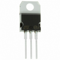
STP5NK40Z STMicroelectronics, STP5NK40Z Datasheet

STP5NK40Z
Specifications of STP5NK40Z
Available stocks
Related parts for STP5NK40Z
STP5NK40Z Summary of contents
Page 1
... ST full range of high voltage MOSFETs in- cluding revolutionary MDmesh™ products. APPLICATIONS HIGH CURRENT, HIGH SPEED SWITCHING IDEAL FOR OFF-LINE POWER SUPPLIES, ADAPTORS AND PFC LIGHTING ORDERING INFORMATION SALES TYPE STP5NK40Z STP5NK40ZFP STD5NK40ZT4 STD5NK40Z-1 February 2003 STP5NK40Z - STP5NK40ZFP STD5NK40Z - STD5NK40Z TO-220/TO-220FP/DPAK/IPAK ...
Page 2
... STP5NK40Z - STP5NK40ZFP - STD5NK40Z - STD5NK40Z-1 ABSOLUTE MAXIMUM RATINGS Symbol Parameter V Drain-source Voltage ( Drain-gate Voltage (R DGR V Gate- source Voltage GS I Drain Current (continuous Drain Current (continuous Drain Current (pulsed Total Dissipation at T TOT Derating Factor V Gate source ESD(HBM-C=100pF, R=1.5K ESD(G-S) dv/dt (1) Peak Diode Recovery voltage slope ...
Page 3
... Reverse Recovery Current RRM Note: 1. Pulsed: Pulse duration = 300 µs, duty cycle 1 Pulse width limited by safe operating area defined as a constant equivalent capacitance giving the same charging time as C oss eq DSS STP5NK40Z - STP5NK40ZFP - STD5NK40Z - STD5NK40Z-1 =25°C UNLESS OTHERWISE SPECIFIED) CASE Test Conditions ...
Page 4
... STP5NK40Z - STP5NK40ZFP - STD5NK40Z - STD5NK40Z-1 Safe Operating Area For TO-220/DPAK/IPAK Thermal Impedance For TO-220/DPAK/IPAK Output Characteristics 4/13 Safe Operating Area For TO-220FP Thermal Impedance For TO-220FP Transfer Characteristics ...
Page 5
... Transconductance Gate Charge vs Gate-source Voltage Normalized Gate Threshold Voltage vs Temp. STP5NK40Z - STP5NK40ZFP - STD5NK40Z - STD5NK40Z-1 Static Drain-source On Resistance Capacitance Variations Normalized On Resistance vs Temperature 5/13 ...
Page 6
... STP5NK40Z - STP5NK40ZFP - STD5NK40Z - STD5NK40Z-1 Source-drain Diode Forward Characteristics Maximum Avalanche Energy vs Temperature 6/13 Normalized BVDSS vs Temperature ...
Page 7
... Fig. 1: Unclamped Inductive Load Test Circuit Fig. 3: Switching Times Test Circuit For Resistive Load Fig. 5: Test Circuit For Inductive Load Switching And Diode Recovery Times STP5NK40Z - STP5NK40ZFP - STD5NK40Z - STD5NK40Z-1 Fig. 2: Unclamped Inductive Waveform Fig. 4: Gate Charge test Circuit 7/13 ...
Page 8
... STP5NK40Z - STP5NK40ZFP - STD5NK40Z - STD5NK40Z-1 DIM. MIN. A 4.40 C 1. 0.49 F 0.61 F1 1.14 F2 1.14 G 4.95 G1 2 13.0 L5 2.65 L6 15.25 L7 6.2 L9 3.5 DIA. 3.75 8/13 TO-220 MECHANICAL DATA mm TYP. MAX. 4.60 1.32 2.72 1.27 0.70 0.88 1.70 1.70 5.15 2.7 10.40 16.4 14 ...
Page 9
... STP5NK40Z - STP5NK40ZFP - STD5NK40Z - STD5NK40Z-1 TO-220FP MECHANICAL DATA mm. DIM. MIN. TYP A 4.4 B 2.5 D 2.5 E 0.45 F 0.75 F1 1.15 F2 1.15 G 4. 28.6 L4 9.8 L5 2 Ø 3 MAX. MIN. 4.6 0.173 2.7 0.098 2.75 0.098 0.7 0.017 1 0.030 1.5 0.045 1.5 0.045 5.2 0.195 2 ...
Page 10
... STP5NK40Z - STP5NK40ZFP - STD5NK40Z - STD5NK40Z-1 DIM. MIN. A 2.20 A1 0.90 A2 0.03 B 0.64 B2 5.20 C 0.45 C2 0.48 D 6.00 E 6.40 G 4. 10/13 TO-252 (DPAK) MECHANICAL DATA mm TYP. MAX. 2.40 1.10 0.23 0.90 5.40 0.60 0.60 6.20 6.60 4.60 10.10 0.8 1. inch MIN. TYP. MAX. 0.087 ...
Page 11
... STP5NK40Z - STP5NK40ZFP - STD5NK40Z - STD5NK40Z-1 TO-251 (IPAK) MECHANICAL DATA mm DIM. MIN. TYP. A 2.2 A1 0.9 A3 0.7 B 0. 0. 6.4 G 4 0.8 L2 0.8 L2 MAX. MIN. 2.4 0.086 1.1 0.035 1.3 0.027 0.9 0.025 5.4 0.204 0.85 0.95 0.6 0.017 0.6 0.019 6 ...
Page 12
... STP5NK40Z - STP5NK40ZFP - STD5NK40Z - STD5NK40Z-1 DPAK FOOTPRINT All dimensions are in millimeters TAPE AND REEL SHIPMENT (suffix ”T4”)* TAPE MECHANICAL DATA mm DIM. MIN. MAX. MIN. A0 6.8 7 0.267 0.275 B0 10.4 10.6 0.409 0.417 B1 12.1 D 1.5 1.6 0.059 0.063 D1 1.5 0.059 E 1.65 1.85 0.065 0.073 F 7 ...
Page 13
... STP5NK40Z - STP5NK40ZFP - STD5NK40Z - STD5NK40Z-1 Information furnished is believed to be accurate and reliable. However, STMicroelectronics assumes no responsibility for the consequences of use of such information nor for any infringement of patents or other rights of third parties which may result from its use. No license is granted by implication or otherwise under any patent or patent rights of STMicroelectronics. Specifications mentioned in this publication are subject to change without notice ...


