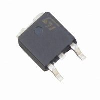
STD90NH02LT4 STMicroelectronics, STD90NH02LT4 Datasheet - Page 9

STD90NH02LT4
Manufacturer Part Number
STD90NH02LT4
Description
MOSFET N-CH 24V 60A DPAK
Manufacturer
STMicroelectronics
Series
STripFET™r
Datasheet
1.STD90NH02LT4.pdf
(16 pages)
Specifications of STD90NH02LT4
Fet Type
MOSFET N-Channel, Metal Oxide
Fet Feature
Logic Level Gate
Rds On (max) @ Id, Vgs
6 mOhm @ 30A, 10V
Drain To Source Voltage (vdss)
24V
Current - Continuous Drain (id) @ 25° C
60A
Vgs(th) (max) @ Id
2.5V @ 250µA
Gate Charge (qg) @ Vgs
64nC @ 10V
Input Capacitance (ciss) @ Vds
2850pF @ 15V
Power - Max
95W
Mounting Type
Surface Mount
Package / Case
DPak, TO-252 (2 leads+tab), SC-63
Lead Free Status / RoHS Status
Lead free / RoHS Compliant
Available stocks
Company
Part Number
Manufacturer
Quantity
Price
Part Number:
STD90NH02LT4
Manufacturer:
ST
Quantity:
20 000
STD90NH02L- STD90NH02L-1
4
Appendix A
The power losses associated with the FETs in a synchronous buck converter can be
estimated using the equations shown in the table below. The formulas give a good
approximation, for the sake of performance comparison, of how different pairs of devices
affect the converter efficiency. However a very important parameter, the working
temperature, is not considered. The real device behavior is really dependent on how the
heat generated inside the devices is removed to allow for a safer working junction
temperature.
●
●
●
●
●
●
●
●
●
●
●
Table 6.
Figure 19. Buck converter: power losses estimation
The low side (SW2) device requires:
Very low R
Small Qgls to reduce the gate charge losses
Small Coss to reduce losses due to output capacitance
Small Qrr to reduce losses on SW1 during its turn-on
The Cgd/Cgs ratio lower than Vth/Vgg ratio especially with low drain to source
voltage to avoid the cross conduction phenomenon;
The high side (SW1) device requires:
Small Rg and Ls to allow higher gate current peak and to limit the voltage feedback on
the gate
Small Qg to have a faster commutation and to reduce gate charge losses
Low R
Pconduction
Pswitching
DS(on)
Power losses calculation
DS(on)
to reduce the conduction losses.
to reduce conduction losses
V
in
*
High side switching (SW1)
(Q
gsth(SW1)
R
DS(on)SW1
+
Q
I *
gd(SW1)
2
L
*
δ
)
f *
*
I
I
L
g
R
Low side switch (SW2)
Zero Voltage Switching
DS(on)SW2
I *
2
L
*
Appendix A
1 (
−
δ
)
9/16


