SPD02N60C3 Infineon Technologies, SPD02N60C3 Datasheet
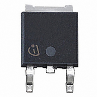
MOSFET N-CH 650V 1.8A DPAK

SPD02N60C3

Manufacturer Part Number
SPD02N60C3
Description
MOSFET N-CH 650V 1.8A DPAK
Manufacturer
Infineon Technologies
Series
CoolMOS™r
Datasheets

Specifications of SPD02N60C3

Fet Type
MOSFET N-Channel, Metal Oxide
Fet Feature
Standard
Rds On (max) @ Id, Vgs
3 Ohm @ 1.1A, 10V
Drain To Source Voltage (vdss)
650V
Current - Continuous Drain (id) @ 25° C
1.8A
Vgs(th) (max) @ Id
3.9V @ 80µA
Gate Charge (qg) @ Vgs
12.5nC @ 10V
Input Capacitance (ciss) @ Vds
200pF @ 25V
Power - Max
25W
Mounting Type
Surface Mount
Package / Case
DPak, TO-252 (2 leads+tab), SC-63
Transistor Polarity
N Channel
Continuous Drain Current Id
1.8A
Drain Source Voltage Vds
650V
On Resistance Rds(on)
3ohm
Rds(on) Test Voltage Vgs
10V
Voltage Vgs Max
20V
Operating Temperature
RoHS Compliant
Threshold Voltage Vgs Typ
3V
Rohs Compliant
Yes
Lead Free Status / RoHS Status
Lead free / RoHS Compliant
Other names
SP000013693
SP000077610
SPD02N60C3INTR
SPD02N60C3T
SPD02N60C3T
SPD02N60C3ZT

Available stocks

Company
Part Number
Manufacturer
Quantity
Price
Part Number:
SPD02N60C3
Manufacturer:
INFINEON
Quantity:
30 000
Part Number:
SPD02N60C3
Manufacturer:
INFINEON/英飞凌
Quantity:
20 000
Company:
Part Number:
SPD02N60C3
Quantity:
7 500
Company:
Part Number:
SPD02N60C3
Quantity:
568
Rev. 2.5
T
T
Gate source voltage static
Reverse diode dv/dt
C
C
V
V
DD
DD
5)
G
G
t
p
T
jmax
P
T
T
jmax
jmax
dv/dt
E
V
V
P
AR
GS
GS
tot
V
G
DS
T
15
jmax
G
8 04-07
V/ns

Related parts for SPD02N60C3

SPD02N60C3 Summary of contents

Page 1

Gate source voltage static 5) Reverse diode dv/dt Rev. 2.5 T jmax jmax T jmax tot dv/ ...

Page 2

TO252: reflow soldering, MSL3; TO251: wavesoldering Rev. 2.5 R thJC R thJA V (BR)DSS ...

Page 3

Transconductance Input capacitance Output capacitance Reverse transfer capacitance Turn-on delay time Rise time Turn-off delay time Fall time Gate to source charge Gate to drain charge 5 I <=I , di/dt<=400A/us DClink Identical low-side and high-side switch. ...

Page 4

Inverse diode direct current, pulsed Reverse recovery time Reverse recovery charge Peak reverse recovery current Rev rrm P 8 04-07 ...

Page 5

T C Rev. 2 8-04-07 ...

Page 6

Rev. 2 04-07 ...

Page 7

max V DS max di/ Rev. 2 04-07 ...

Page 8

Rev. 2.5 dv/ 04- ...

Page 9

(BR)DSS j Rev. 2 04-07 ...

Page 10

Rev. 2.5 C oss 04-07 ...

Page 11

... PG-TO-252-3-1 (D-PAK), PG-TO-252-3-11 (D-PAK), PG-TO-252-3-21 (D-PAK) Rev. 2.5 Page 11 SPD02N60C3 SPU02N60C3 2008-04-07 ...

Page 12

... PG-TO-251-3-1 (I-PAK), PG-TO-251-3-21 (I-PAK) Rev. 2.5 Page 12 SPD02N60C3 SPU02N60C3 2008-04-07 ...

Page 13

... Rev. 2 SPD02N60C3 SPU02N60C3 8 04-07 ...

Related keywords