BSS138LT1 ON Semiconductor, BSS138LT1 Datasheet
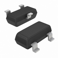
MOSFET N-CH 50V 200MA SOT-23

BSS138LT1

Manufacturer Part Number
BSS138LT1
Description
MOSFET N-CH 50V 200MA SOT-23
Manufacturer
ON Semiconductor
Datasheet

Specifications of BSS138LT1

Fet Type
MOSFET N-Channel, Metal Oxide
Fet Feature
Logic Level Gate
Rds On (max) @ Id, Vgs
3.5 Ohm @ 200mA, 5V
Drain To Source Voltage (vdss)
50V
Current - Continuous Drain (id) @ 25° C
200mA
Vgs(th) (max) @ Id
1.5V @ 1mA
Input Capacitance (ciss) @ Vds
50pF @ 25V
Power - Max
225mW
Mounting Type
Surface Mount
Package / Case
SOT-23-3, TO-236-3, Micro3™, SSD3, SST3
Lead Free Status / RoHS Status
Contains lead / RoHS non-compliant
Gate Charge (qg) @ Vgs
-
Other names
BSS138LT1OSCT

Available stocks

Company
Part Number
Manufacturer
Quantity
Price
Part Number:
BSS138LT1
Manufacturer:
ON/安森美
Quantity:
20 000
Part Number:
BSS138LT1G
Manufacturer:
ON
Quantity:
6 000
Part Number:
BSS138LT1G
Manufacturer:
ON
Quantity:
30 000
Part Number:
BSS138LT1G
Manufacturer:
ON
Quantity:
464
Part Number:
BSS138LT1G
Manufacturer:
ON
Quantity:
8 000
Part Number:
BSS138LT1G
Manufacturer:
ON/安森美
Quantity:
20 000
Part Number:
BSS138LT1G
0
Company:
Part Number:
BSS138LT1G
Quantity:
3 372
Company:
Part Number:
BSS138LT1G
Quantity:
4 500
Company:
Part Number:
BSS138LT1G
Quantity:
1 350
BSS138LT1
Power MOSFET
200 mA, 50 V
N−Channel SOT−23
portable and battery−powered products such as computers, printers,
PCMCIA cards, cellular and cordless telephones.
Features
Stresses exceeding Maximum Ratings may damage the device. Maximum
Ratings are stress ratings only. Functional operation above the Recommended
Operating Conditions is not implied. Extended exposure to stresses above the
Recommended Operating Conditions may affect device reliability.
© Semiconductor Components Industries, LLC, 2009
February, 2009 − Rev. 5
MAXIMUM RATINGS
Drain−to−Source Voltage
Gate−to−Source Voltage − Continuous
Drain Current
Total Power Dissipation @ T
Operating and Storage Temperature
Thermal Resistance,
Maximum Lead Temperature for
Typical applications are DC−DC converters, power management in
Low Voltage Applications
Low Threshold Voltage (V
Miniature SOT−23 Surface Mount Package Saves Board Space
Pb−Free Packages are Available
Range
Junction−to−Ambient
Soldering Purposes, for 10 seconds
− Continuous @ T
− Pulsed Drain Current (t
Rating
A
= 25°C
(T
A
= 25°C unless otherwise noted)
p
A
Preferred Device
≤ 10 ms)
= 25°C
GS(th)
: 0.5 V−1.5 V) Makes it Ideal for
Symbol
T
V
R
J
V
I
P
, T
DSS
DM
T
I
qJA
GS
D
D
L
stg
− 55 to 150
Value
± 20
200
800
225
556
260
50
1
°C/W
Unit
mW
Vdc
Vdc
mA
°C
°C
†For information on tape and reel specifications,
Preferred devices are recommended choices for future use
and best overall value.
BSS138LT1
BSS138LT1G
BSS138LT3
BSS138LT3G
including part orientation and tape sizes, please
refer to our Tape and Reel Packaging Specifications
Brochure, BRD8011/D.
*Date Code orientation and/or overbar may
vary depending upon manufacturing location.
1
Device
J1
M
G
(Note: Microdot may be in either location)
CASE 318
STYLE 21
SOT−23
ORDERING INFORMATION
2
1
R
http://onsemi.com
200 mA, 50 V
= Device Code
= Date Code*
= Pb−Free Package
DS(on)
3
(Pb−Free)
(Pb−Free)
Package
SOT−23
SOT−23
SOT−23
SOT−23
N−Channel
Publication Order Number:
= 3.5 W
3
2
1
10,000 Tape & Reel
10,000 Tape & Reel
3000 Tape & Reel
3000 Tape & Reel
MARKING
DIAGRAM
J1 M G
Shipping
BSS138LT1/D
G

Related parts for BSS138LT1

BSS138LT1 Summary of contents

Page 1

... SOT−23 3000 Tape & Reel (Pb−Free) SOT−23 10,000 Tape & Reel SOT−23 10,000 Tape & Reel (Pb−Free) including part orientation and tape sizes, please refer to our Tape and Reel Packaging Specifications Brochure, BRD8011/D. Publication Order Number: BSS138LT1/D † ...

Page 2

ELECTRICAL CHARACTERISTICS Characteristic OFF CHARACTERISTICS Drain−to−Source Breakdown Voltage ( Vdc 250 mAdc Zero Gate Voltage Drain Current ( Vdc Vdc Vdc ...

Page 3

TYPICAL ELECTRICAL CHARACTERISTICS 0 3 25° 0.7 0.6 0.5 0.4 0.3 0.2 0 DRAIN-TO-SOURCE VOLTAGE (VOLTS) DS Figure 1. On−Region Characteristics 2.2 2 ...

Page 4

TYPICAL ELECTRICAL CHARACTERISTICS 2 0.05 0.1 0. DRAIN CURRENT (AMPS) D Figure 7. On−Resistance versus Drain Current 4 ...

Page 5

... ON Semiconductor Website: www.onsemi.com Order Literature: http://www.onsemi.com/orderlit For additional information, please contact your local Sales Representative BSS138LT1/D ...

Related keywords