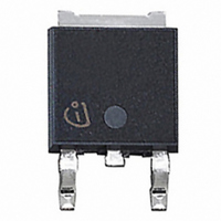
SPD30N03S2L10T Infineon Technologies, SPD30N03S2L10T Datasheet

SPD30N03S2L10T
Specifications of SPD30N03S2L10T
Related parts for SPD30N03S2L10T
SPD30N03S2L10T Summary of contents
Page 1
OptiMOS ® Power-Transistor Feature • N-Channel • Enhancement mode • Logic Level • Low On-Resistance R DS(on) • Excellent Gate Charge x R • Superior thermal resistance • 175°C operating temperature • Avalanche rated • dv/dt rated Type Package SPD30N03S2L-10 ...
Page 2
Thermal Characteristics Parameter Characteristics Thermal resistance, junction - case Thermal resistance, junction - ambient, leaded SMD version, device on PCB: @ min. footprint cooling area Electrical Characteristics Parameter Static Characteristics Drain-source breakdown voltage ...
Page 3
Electrical Characteristics Parameter Dynamic Characteristics Transconductance Input capacitance Output capacitance Reverse transfer capacitance Turn-on delay time Rise time Turn-off delay time Fall time Gate Charge Characteristics Gate to source charge Gate to drain charge Gate charge total Gate plateau voltage ...
Page 4
Power dissipation tot C ≥ parameter SPD30N03S2L-10 110 100 120 140 160 3 Safe ...
Page 5
Typ. output characteristic =25° parameter µs p SPD30N03S2L- 100W tot ...
Page 6
Drain-source on-state resistance DS(on) j parameter : SPD30N03S2L-10 24 mΩ 98% 10 typ -60 ...
Page 7
Typ. avalanche energy par 160 mJ 120 100 105 15 Drain-source ...
Page 8
... For information on the types in question please contact your nearest Infineon Technologies Office. Infineon Technologies Components may only be used in life-support devices or systems with the express written approval of Infineon Technologies failure of such components can reasonably be expected to cause the failure of that life-support device or system affect the safety or effectiveness of that device or system Life support devices or systems are intended to be implanted in the human body support and/or maintain and sustain and/or protect human life ...


