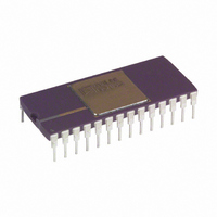
AD676BD Analog Devices Inc, AD676BD Datasheet

AD676BD
Specifications of AD676BD
Available stocks
Related parts for AD676BD
AD676BD Summary of contents
Page 1
FEATURES Autocalibrating On-Chip Sample-Hold Function Parallel Output Format 16 Bits No Missing Codes 1 LSB INL –97 dB THD 90 dB S/(N+D) 1 MHz Full Power Bandwidth PRODUCT DESCRIPTION The AD676 is a multipurpose 16-bit parallel output analog-to- digital ...
Page 2
AD676–SPECIFICATIONS AC SPECIFICATIONS ( MIN Parameter 2 Total Harmonic Distortion (THD kSPS MIN MAX @ 100 kSPS, + 100 kSPS MIN MAX Signal-to-Noise and Distortion Ratio (S/(N+D)) @ ...
Page 3
DC SPECIFICATIONS ( MIN Parameter TEMPERATURE RANGE J, K Grades A, B Grades ACCURACY Resolution Integral Nonlinearity (INL kSPS MIN MAX @ 100 kSPS, + 100 kSPS MIN ...
Page 4
AD676 TIMING SPECIFICATIONS (T Parameter 2 Conversion Time 3 CLK Period Calibration Time Sampling Time (Included CAL to BUSY Delay BUSY to SAMPLE Delay SAMPLE to BUSY Delay 4 CLK HIGH 4 CLK LOW SAMPLE LOW ...
Page 5
... Model Temperature Range AD676JD +70 C AD676KD +70 C AD676AD – +85 C AD676BD – +85 C NOTES 1 For details on grade and package offerings screened in accordance with MIL-STD-883, refer to the AD676/883 data sheet Ceramic DIP. ABSOLUTE MAXIMUM RATINGS AGND . . . . . . . . . . . . . . . . . . . . . . . . –0 + AGND . . . . . . . . . . . . . . . . . . . . . . . . – +0 AGND to DGND . . . . . . . . . . . . . . . . . . . . . . . . . . . . ...
Page 6
AD676 Pin Name Type 1–6 BIT 11-BIT BUSY DO 8 CAL DI 9 SAMPLE DI 10 CLK DI 11 DGND AGND P/AI 14 AGND SENSE ...
Page 7
NYQUIST FREQUENCY An implication of the Nyquist sampling theorem, the “Nyquist frequency” converter is that input frequency which is one half the sampling frequency of the converter. TOTAL HARMONIC DISTORTION Total harmonic distortion (THD) is the ratio of ...
Page 8
AD676 FUNCTIONAL DESCRIPTION The AD676 is a multipurpose 16-bit analog-to-digital converter and includes circuitry which performs an input sample/hold function, ground sense, and autocalibration. These functions are segmented onto two monolithic chips—an analog signal pro- cessor and a digital controller. ...
Page 9
CONTINUOUS CONVERSION For maximum throughput rate, the AD676 can be operated in a continuous convert mode (see Figure 2b). This is accomplished by utilizing the fact that SAMPLE will no longer be ignored af- ter BUSY goes LOW ...
Page 10
AD676 POWER SUPPLIES AND DECOUPLING The AD676 has three power supply input pins. V provide the supply voltages to operate the analog portions of the AD676 including the ADC and sample-hold amplifier (SHA). V provides the supply voltage which operates ...
Page 11
Using AGND SENSE to remotely sense the ground potential of the signal source can be useful if the signal has to be carried some distance to the A/D converter. Since all IC ground cur- rents have to return to the ...
Page 12
AD676 AD586 output, thereby optimizing the overall performance of the AD676 recommended that high qual- ity tantalum capacitor be tied between the V AD676 and ground to minimize the impedance on the ...
Page 13
AC PERFORMANCE AC parameters, which include S/(N+D), THD, etc., reflect the AD676’s effect on the spectral content of the analog input sig- nal. Figures 12 through 16 provide information on the AD676’s ac performance under a variety of conditions. As ...
Page 14
AD676 MICROPROCESSOR INTERFACE The AD676 is ideally suited for use in both traditional dc mea- surement applications supporting a microprocessor, and in ac signal processing applications interfacing to a digital signal pro- cessor. The AD676 is designed to interface with ...
Page 15
THD S/(N+ 2.5 3.5 4.5 5.5 6.5 7.5 V – Volts REF Figure 12. S/(N+D) and THD vs. V Figure 14. 4096 Point FFT at 96 kSPS, f ...
Page 16
AD676 0.005 (0.13) MIN 28 1 0.225 (5.72) MAX 0.026 (0.66) 0.200 (5.08) 0.125 (3.18) 0.014 (0.36) OUTLINE DIMENSIONS Dimensions shown in inches and (mm). 28-Pin Ceramic DIP Package (D-28) 0.100 (2.54) MAX 15 14 1.490 (37.85) MAX 0.060 (1.52) ...


