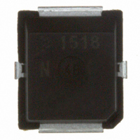
MRF1518NT1 Freescale Semiconductor, MRF1518NT1 Datasheet

MRF1518NT1
Specifications of MRF1518NT1
MRF1518NT1TR
Available stocks
Related parts for MRF1518NT1
MRF1518NT1 Summary of contents
Page 1
... BROADBAND RF POWER MOSFET CASE 466 - 03, STYLE 1 PLD - 1.5 PLASTIC Symbol Value V - 0.5, +40 DSS V ± 62 +150 stg T 150 J (2) Symbol Value R 2 θJC Package Peak Temperature 260 MRF1518NT1 Unit Vdc Vdc Adc W W/°C °C °C Unit °C/W Unit °C 1 ...
Page 2
... DS GS Functional Tests (In Freescale Test Fixture) Common - Source Amplifier Power Gain (V = 12.5 Vdc Watts 150 mA 520 MHz) DD out DQ Drain Efficiency (V = 12.5 Vdc Watts 150 mA 520 MHz) DD out DQ MRF1518NT1 2 = 25°C unless otherwise noted) Symbol I DSS I GSS V GS(th) V DS(on) C iss C oss C rss G ps η ...
Page 3
... Microstrip 1.113″ x 0.080″ Microstrip 0.433″ x 0.080″ Microstrip ® Glass Teflon , 31 mils, 2 oz. Copper V = 12.5 Vdc DD 470 MHz 500 MHz 450 MHz 520 MHz OUTPUT POWER (WATTS) out Figure 3. Input Return Loss versus Output Power MRF1518NT1 ...
Page 4
... I , BIASING CURRENT (mA) DQ Figure 6. Output Power versus Biasing Current 12 470 MHz 520 MHz 5 500 MHz SUPPLY VOLTAGE (VOLTS) DD Figure 8. Output Power versus Supply Voltage MRF1518NT1 12.5 Vdc Figure 5. Drain Efficiency versus Output Power 70 470 MHz 65 450 MHz 12.5 Vdc ...
Page 5
... Microstrip 0.104″ x 0.080″ Microstrip 1.759″ x 0.080″ Microstrip ® Glass Teflon , 31 mils, 2 oz. Copper V = 12.5 Vdc DD 850 MHz 820 MHz 830 MHz OUTPUT POWER (WATTS) out Figure 12. Input Return Loss versus Output Power MRF1518NT1 C15 RF OUTPUT 840 MHz ...
Page 6
... I , BIASING CURRENT (mA) DQ Figure 15. Output Power versus Biasing Current 12 11 840 MHz 850 MHz SUPPLY VOLTAGE (VOLTS) DD Figure 17. Output Power versus Supply Voltage MRF1518NT1 6 80 840 MHz 12.5 Vdc Figure 14. Drain Efficiency versus Output 70 60 850 MHz 12.5 Vdc ...
Page 7
... Microstrip 0.806″ x 0.080″ Microstrip 0.553″ x 0.080″ Microstrip ® Glass Teflon , 31 mils, 2 oz. Copper V = 12.5 Vdc DD 440 MHz 400 MHz 470 MHz OUTPUT POWER (WATTS) out Figure 21. Input Return Loss versus Output Power MRF1518NT1 ...
Page 8
... MHz 200 400 600 I , BIASING CURRENT (mA) DQ Figure 24. Output Power versus Biasing Current 12 440 MHz 470 MHz SUPPLY VOLTAGE (VOLTS) DD Figure 26. Output Power versus Supply Voltage MRF1518NT1 12.5 Vdc Figure 23. Drain Efficiency versus Output 12.5 Vdc 26.8 dBm in 30 800 ...
Page 9
... Microstrip 0.305″ x 0.080″ Microstrip 0.155″ x 0.080″ Microstrip ® Glass Teflon , 31 mils, 2 oz. Copper V = 12.5 Vdc DD 155 MHz 135 MHz 175 MHz OUTPUT POWER (WATTS) out Figure 30. Input Return Loss versus Output Power MRF1518NT1 RF OUTPUT ...
Page 10
... MHz 155 MHz 200 400 600 I , BIASING CURRENT (mA) DQ Figure 33. Output Power versus Biasing Current SUPPLY VOLTAGE (VOLTS) DD Figure 35. Output Power versus Supply Voltage MRF1518NT1 12.5 Vdc Figure 32. Drain Efficiency versus Output 70 175 MHz 12.5 Vdc 24.5 dBm 800 ...
Page 11
... JUNCTION TEMPERATURE (°C) J This above graph displays calculated MTTF in hours x ampere drain current. Life tests at elevated temperatures have correlated to better than ±10% of the theoretical prediction for metal failure. Divide 2 MTTF factor by I for MTTF in a particular application. D 190 200 210 2 MRF1518NT1 11 ...
Page 12
... Figure 1 Complex conjugate of the load OL impedance at given output power, voltage, frequency, and η > Note was chosen based on tradeoffs between gain, drain efficiency, and device stability. OL Figure 38. Series Equivalent Input and Output Impedance MRF1518NT1 Ω 850 MHz f = 850 MHz 820 MHz V MHz ...
Page 13
... Figure 28 Complex conjugate of the load OL impedance at given output power, > voltage, frequency, and η D Input Device Matching Under Test Network 150 mA out Ω Ω 18.31 - j0.76 8.97 +j2.62 17.72 +j1.85 9.69 +j2.81 18.06 +j5.23 7.94 +j1.14 > Output Matching Network MRF1518NT1 13 ...
Page 14
... MRF1518NT1 14 = 12.5 Vdc 150 ∠ φ 18.91 99 0.033 9.40 86 0.033 4.47 73 0.026 2. ...
Page 15
... DS(on) ALC/AGC and modulation systems. This characteristic is very dependent on frequency and load line. has a positive temperature DS(on) DSS can result in permanent GS ), whose value is application dependent 150 mA, which is the DQ DQ MRF1518NT1 is not 9 Ω may 15 ...
Page 16
... Impedance matching networks similar to those used with bipolar transistors are suitable for this device. For examples see Freescale Application Note AN721, “Impedance Matching Networks Applied to RF Power Transistors.” MRF1518NT1 16 Large - signal impedances are provided, and will yield a good first pass approximation. ...
Page 17
... S 0.006 0.012 0.15 U 0.006 0.012 0.15 ZONE V 0.000 0.021 0.00 ZONE W 0.000 0.010 0.00 ZONE X 0.000 0.010 0.00 MRF1518NT1 0.115 2.92 inches mm MAX 6.73 5.97 1.83 3.81 0.66 1.12 1.78 1.60 4.57 7.24 6.48 6.10 0.20 1.60 5.33 0.31 ...
Page 18
... June 2009 • Modified data sheet to reflect MSL rating change from result of the standardization of packing process as described in Product and Process Change Notification number, PCN13516 • Added Electromigration MTTF Calculator availability to Product Documentation, Tools and Software MRF1518NT1 18 REVISION HISTORY Description RF Device Data ...
Page 19
... Freescale Semiconductor was negligent regarding the design or manufacture of the part. Freescalet and the Freescale logo are trademarks of Freescale Semiconductor, Inc. All other product or service names are the property of their respective owners. © Freescale Semiconductor, Inc. 2008-2009. All rights reserved. MRF1518NT1 19 ...


