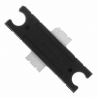
MRF6V2010NBR5 Freescale Semiconductor, MRF6V2010NBR5 Datasheet

MRF6V2010NBR5
Specifications of MRF6V2010NBR5
Available stocks
Related parts for MRF6V2010NBR5
MRF6V2010NBR5 Summary of contents
Page 1
... MTTF calculator available at http://www.freescale.com/rf. Select Software & Tools/Development Tools/Calculators to access MTTF calculators by product. 3. Refer to AN1955, Thermal Measurement Methodology of RF Power Amplifiers http://www.freescale.com/rf. Select Documentation/Application Notes -- AN1955. © Freescale Semiconductor, Inc., 2007--2008, 2010. All rights reserved. RF Device Data Freescale Semiconductor = 50 Volts, I ...
Page 2
... Vdc — — 50 μAdc — — 2 1.68 3 Vdc 1.5 2.68 3.5 Vdc — 0.26 — Vdc — 0.13 — pF — 7.3 — pF — 16.3 — 220 MHz, CW out 22.5 23.9 25 — % — --14 -- Device Data Freescale Semiconductor ...
Page 3
... V Chip Capacitors C9 0.6--4.5 pF Variable Capacitor, Gigatrim C10 12 pF Chip Capacitor C16 470 μ Electrolytic Capacitor C17 27 pF Chip Capacitor L1 17.5 nH Inductor L2 Inductors R1 120 Ω, 1/4 W Chip Resistor RF Device Data Freescale Semiconductor C10 DUT Z7 0.062″ x 0.270″ Microstrip Z8 0.198″ ...
Page 4
... MRF6V2010N/NB Rev. 3 Figure 2. MRF6V2010NR1(NBR1) Test Circuit Component Layout MRF6V2010NR1 MRF6V2010NBR1 C12 R1 C11 C8 L1 C10 C9 C14 B2 C13 C15 L2 C16 C18 C17 L3 RF Device Data Freescale Semiconductor ...
Page 5
... DRAIN VOLTAGE (VOLTS) Figure 5. DC Drain Current versus Drain Voltage -- -- --40 -- 220 MHz 220.1 MHz -- Two--Tone Measurements DQ 100 kHz Tone Spacing -- OUTPUT POWER (WATTS) PEP out Figure 7. Third Order Intermodulation Distortion versus Output Power RF Device Data Freescale Semiconductor TYPICAL CHARACTERISTICS 100 ...
Page 6
... Software & Tools/Development Tools/Calculators to access MTTF calculators by product. Figure 13. MTTF versus Junction Temperature T = --30_C C 85_C 25_C Vdc 220 MHz INPUT POWER (dBm 25_C 63 54 85_C 130 150 170 190 210 230 T , JUNCTION TEMPERATURE (° Vdc CW, and η = 62%. DD out D RF Device Data Freescale Semiconductor 25 250 ...
Page 7
... Figure 14. Series Equivalent Source and Load Impedance RF Device Data Freescale Semiconductor Z source f = 220 MHz Vdc mA out f Z source MHz Ω 220 20 + j25 75 + j44 Z = Test circuit impedance as measured from source gate to ground Test circuit impedance as measured load from drain to ground. Input Device ...
Page 8
... CuClad 250GX--0300--55--22, 0.030″, ε C16 B2 C15 L5 C17 C18 C19 L4 L3 130 MHz Rev. 1 Part Number Manufacturer Fair--Rite ATC Johanson ATC Kemet Kemet ATC ATC Kemet Kemet ATC Multicomp CoilCraft CoilCraft CoilCraft CoilCraft Vishay Arlon = 2. Device Data Freescale Semiconductor ...
Page 9
... Chip Capacitors C19 470 μ Electrolytic Capacitor C20 47 μ Electrolytic Capacitor L1 17.5 nH Inductor L2 Inductors L3 5.0 nH Inductor R1 120 Ω, 1/4 W Chip Resistor PCB PCB Material 0.030” RF Device Data Freescale Semiconductor C6 C7 C11 Description 2743021447 ATC100B241JT200XT ATC100B100JT500XT C1825C225J5RAC CDR33BX104AKYM ATC200B223KT50XT ATC200B393KT50XT T491X226K035AT ...
Page 10
... CuClad 250GX--0300--55--22, 0.030″, ε C20 B2 C19 L6 C21 C17 C15 C14 64 MHz Rev. 1 Part Number Manufacturer Fair--Rite ATC ATC ATC Kemet Kemet Kemet ATC ATC Kemet Kemet ATC ATC Multicomp CoilCraft CoilCraft CoilCraft Vishay Arlon = 2. Device Data Freescale Semiconductor ...
Page 11
... MHz Z source f = 220 MHz Z Figure 18. Series Equivalent Source and Load Impedance RF Device Data Freescale Semiconductor Ω o source f = 130 MHz Z source MHz Z source Vdc mA out f Z source MHz Ω 64 37.5 + j15.1 94.5 + j16.7 130 26.7 + j21.3 83.8 + j35.0 220 20.0 + j25.4 75 ...
Page 12
... RF Device Data Freescale Semiconductor ...
Page 13
... MHz |S | ∠ φ 11 800 0.858 --139.7 820 0.861 --140.7 840 0.864 --141.6 860 0.867 --142.6 880 0.870 --143.5 900 0.873 --144.5 RF Device Data Freescale Semiconductor 50 OHM TYPICAL CHARACTERISTICS ( mA 25°C, 50 Ohm System) (continued ∠ φ 1.697 40.2 0.00839 1.636 38.9 0.00818 1 ...
Page 14
... MRF6V2010NR1 MRF6V2010NBR1 14 PACKAGE DIMENSIONS RF Device Data Freescale Semiconductor ...
Page 15
... RF Device Data Freescale Semiconductor MRF6V2010NR1 MRF6V2010NBR1 15 ...
Page 16
... MRF6V2010NR1 MRF6V2010NBR1 16 RF Device Data Freescale Semiconductor ...
Page 17
... RF Device Data Freescale Semiconductor MRF6V2010NR1 MRF6V2010NBR1 17 ...
Page 18
... MRF6V2010NR1 MRF6V2010NBR1 18 RF Device Data Freescale Semiconductor ...
Page 19
... RF Device Data Freescale Semiconductor MRF6V2010NR1 MRF6V2010NBR1 19 ...
Page 20
... MRF6V2010NR1 MRF6V2010NBR1 20 REVISION HISTORY Description and Z values, Fig. 13, Series Equivalent Source and Load source load test condition to indicate AC stimulus on the V iss (37.5 + j15.1) and Z (94.5 + j16.7) 64 MHz values and replotted both source load connection versus the V connection Device Data Freescale Semiconductor ...
Page 21
... Freescale Semiconductor product could create a situation where personal injury or death may occur. Should Buyer ...


